Incorporation of nitrogen into high k dielectric film

a dielectric film and nitrogen technology, applied in the field of thin dielectric films, can solve the problems of long overall deposition time, reduced throughput and consequently greater fabrication cost, and the semiconductor industry is very sensitive to fabrication cos

Inactive Publication Date: 2005-09-29
ASM IP HLDG BV
View PDF75 Cites 412 Cited by
  • Summary
  • Abstract
  • Description
  • Claims
  • Application Information

AI Technical Summary

Benefits of technology

[0020] In accordance with another aspect of the invention, a dielectric layer is provided in an integrated circuit. The dielectric layer comprises a metal oxide throughout a thickness of the dielectric layer, which metal oxide has a dielectric constant greater than about 7. The diele

Problems solved by technology

Slow nucleation entails longer overall deposition times, lower throughput and consequently greater fabrication costs.
The semiconductor industry is very sensitive to fabrication costs.
Accordingly, any increase in wafer throughput, at any stage of processing, translates to reduced production costs and higher margins.
This additional step unfortunately complicates the process flow, requires adjustment of the doping concentrations at the dielectric-electrode interface to ensure the desired work function for the transistor, and does not necessarily guarantee rapid and uniform nucleation.
Ultrathin gate oxides (less than 7 nm), however, have been found to exhibit high defect densities, including pinholes, charge trapping states, and susceptibility to hot carrier injection effects.
Such high defect densities lead to leakage currents through the gate dielectric and rapid device breakdown unacceptable for circuit designs with less than 0.25 μm gate spacing, i.e., sub-quarter-micron technology.
While care under laboratory conditions can be used to control defect densities, such control has been difficult to achieve under commercial volume fabrication conditions.
Moreover, even if the integrity of the oxide i

Method used


Image

  • Incorporation of nitrogen into high k dielectric film
  • Incorporation of nitrogen into high k dielectric film
  • Incorporation of nitrogen into high k dielectric film

Examples


Embodiment Construction

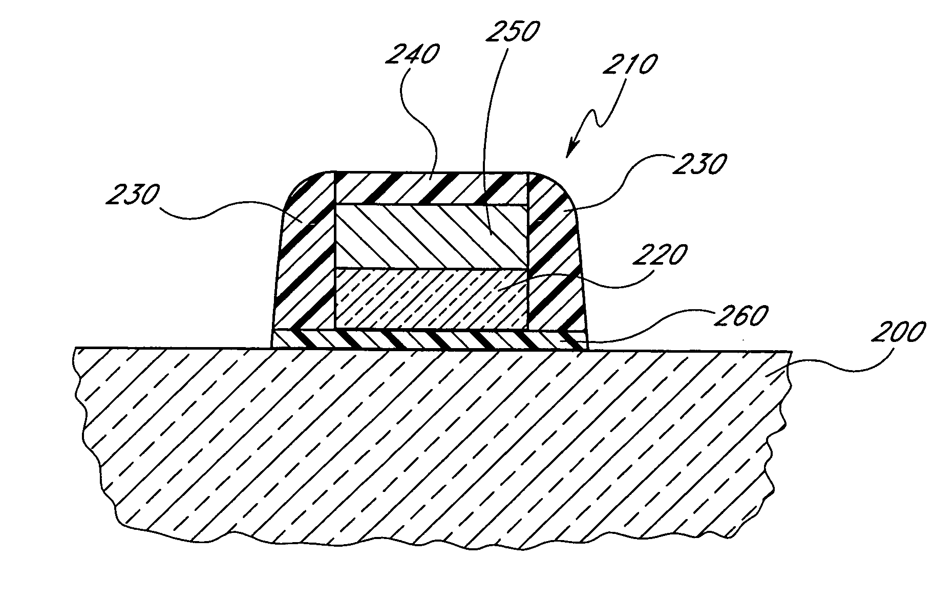
[0033] While the preferred embodiments are described in the context of transistor gate stacks, the skilled artisan will readily appreciate that the principles disclosed herein have application to a variety of contexts in which thin high k materials require a graded composition, particularly those having special interface needs. An example of such a context is in the formation of capacitors including high k dielectrics, proposed for high density memory cells in random access memory (RAM) arrays. The methods described herein are particularly advantageous for maintaining the stability of and preventing diffusion to or from high k materials.

[0034] Conventional gate electrode deposition over high k gate dielectrics has been found to result in poor electrical performance of the resultant devices. In order to increase the reliability and yield of the integrated circuits including high k dielectrics, the present invention provides a varied composition for a high k dielectric, whereby nitro...


PUM

PropertyMeasurementUnit
Thicknessaaaaaaaaaa
Percent by atomaaaaaaaaaa

Abstract

A high k dielectric film and methods for forming the same are disclosed. The high k material includes two peaks of impurity concentration, particularly nitrogen, such as at a lower interface and upper interface, making the layer particularly suitable for transistor gate dielectric applications. The methods of formation include low temperature processes, particularly CVD using a remote plasma generator and atomic layer deposition using selective incorporation of nitrogen in the cyclic process. Advantageously, nitrogen levels are tailored during the deposition process and temperatures are low enough to avoid interdiffusion and allow maintenance of the desired impurity profile.

Description

REFERENCE TO RELATED APPLICATIONS [0001] The present application claims priority under 35 U.S.C. §120 as a divisional of U.S. application Ser. No. 10 / 260,370, filed Sep. 26, 2002, and under 35 U.S.C. §119(e) to U.S. provisional application No. 60 / 326,830, filed Oct. 2, 2001, each of which is incorporated by reference herein.FIELD OF THE INVENTION [0002] The present invention relates generally to thin dielectric films in integrated circuits, and more particularly to nitrogen incorporation into high k gate dielectric films. BACKGROUND OF THE INVENTION [0003] Integrated circuit design is constantly being scaled down in pursuit of faster circuit operation and lower power consumption. Scaled dimensions in a circuit design generally requires attendant changes in fabrication processing. [0004] A basic building block of integrated circuits is the thin film transistor (TFT). As is known in the art, the transistor typically includes a gate electrode separated from a semiconductor layer or sub...

Claims


Application Information

Patent Timeline
IPC IPC(8): C23C16/30C23C16/452C23C16/455H01L21/28C23C16/40H01L21/314H01L21/316H01L21/318H01L29/51
CPCC23C16/308Y10T428/12021C23C16/455H01L21/28017H01L21/28185H01L21/28194H01L21/28202H01L21/3144H01L21/31604H01L21/31683H01L21/318H01L29/517H01L29/518Y10S438/932H01L2924/0002C23C16/452Y10T428/12458H01L2924/00Y10T428/31678H01L21/02189H01L21/02183H01L21/0228H01L21/02181H01L21/02197H01L21/02192H01L21/02178
Inventor SHERO, ERIC J.POMAREDE, CHRISTOPHE
Owner ASM IP HLDG BV
Why Eureka
Try Eureka