Organic element for electroluminescent devices

a technology of electroluminescent devices and organic elements, which is applied in the direction of organic semiconductor devices, discharge tube luminescnet screens, natural mineral layered products, etc., can solve the problems of low oxidation potential of materials, thermal instability, and inability to meet the requirements of many applications, and achieve long operating lifetime and high luminance

Inactive Publication Date: 2005-09-29
EASTMAN KODAK CO
View PDF5 Cites 11 Cited by
  • Summary
  • Abstract
  • Description
  • Claims
  • Application Information

AI Technical Summary

Benefits of technology

[0016] The invention also provides a display and area lighting device incorporating the device and a process for emitting light employing the device. Embodiments of the invention provide a desired high luminance and long operating lifetimes

Problems solved by technology

While organic electroluminescent (EL) devices have been known for over two decades, their performance limitations have represented a barrier to many desirable applications.
Many of these materials contain 1,4-diamines, which can cause the materials to have low oxidation potentials and in some cases to be thermally unstable.
However, is some cases these materials can give unacceptable stability.
That is, the operating lifetimes of devices using these materials may be shorter than desirable.

Method used


Image

  • Organic element for electroluminescent devices
  • Organic element for electroluminescent devices
  • Organic element for electroluminescent devices

Examples


synthesis example 1

Preparation of Inv-7

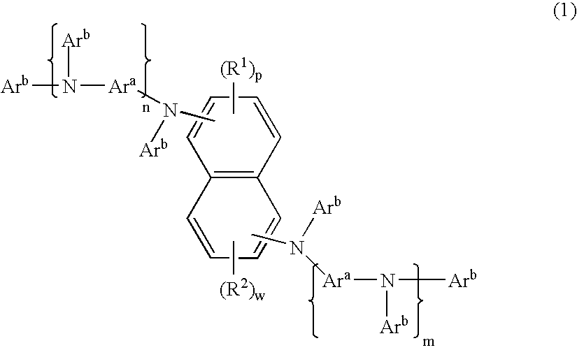
[0152] N,N,N′-Triphenyl-1,5-diaminonaphthalene was prepared by combining 1,5-Diaminonaphthalene (16.0 g, 0.101 mol) with bromobenzene (47.1 g, 0.300 mol), palladium diacetate (1.2 g, 0.004 mol), tri-t-butylphosphine (4 mL), sodium t-butoxide (24.0g, 0.26 mol), and xylene (400 mL). The mixture was heated at 140° C. with magnetic stirring under a nitrogen atmosphere. After 15 h, an additional amount of palladium diacetate (0.100 g, 0.0004 mol) was added. After heating for another 6 h, more palladium diacetate (0.100 g, 0.0004 mol) was added. After heating for another 15 h the heat was removed. After cooling to room temperature, the solid present was filtered off and the filtrate was purified by column chromatography. This afforded 6.0 g (15% yield) of N,N,N′-triphenyl-1,5-diaminonaphthalene.

[0153] 1,5-dibromo-2,6-di-t-butylnapthalene was prepared from 2,6-Di-t-butylnaphthalene (see R. Harvey, J. Pataki, C. Cortez, P. Di Raddo, C. Yang, J. Org. Chem., 56, 1210 (19...

synthesis example 2

Preparation of Inv-1

[0155] Compound Inv-1 was prepared by combining N-α-naphthyl, N-β-naphthylamine (2.0 g, 7.4 mmol), 1,5-dibromo-2,6-di-t-butylnaphthalene (1.5 g, 3.77 mmol) palladium diacetate (0.110 g, 0.5 mmol), tri-t-butylphosphine (ca. 0.4 mL), sodium t-butoxide (0.85 g, 9.2 mmol), and toluene (40 mL) in a 100 mL round-bottomed-flask under nitrogen and with magnetic stirring. The reaction mixture was heated at reflux and after 1 h, 0.4 mL of tri-t-butylphosphine was added and heating was continued, after a total of 4 h, 150 mg of palladium diacetate was added and the reaction mixture was heated for 16 h. Palladium diacetate (150 mg) was added and heating was continued for 3.5 h. The heat was removed and the reaction mixture was stirred for 60 h. Palladium diacetate (50 mg) was then added and the reaction mixture was heated at reflux for 4 h. The heat was removed and, after cooling, solid material was filtered off. The filtrate was evaporated and the solid obtained was dissol...

example 1

DEVICE EXAMPLE 1

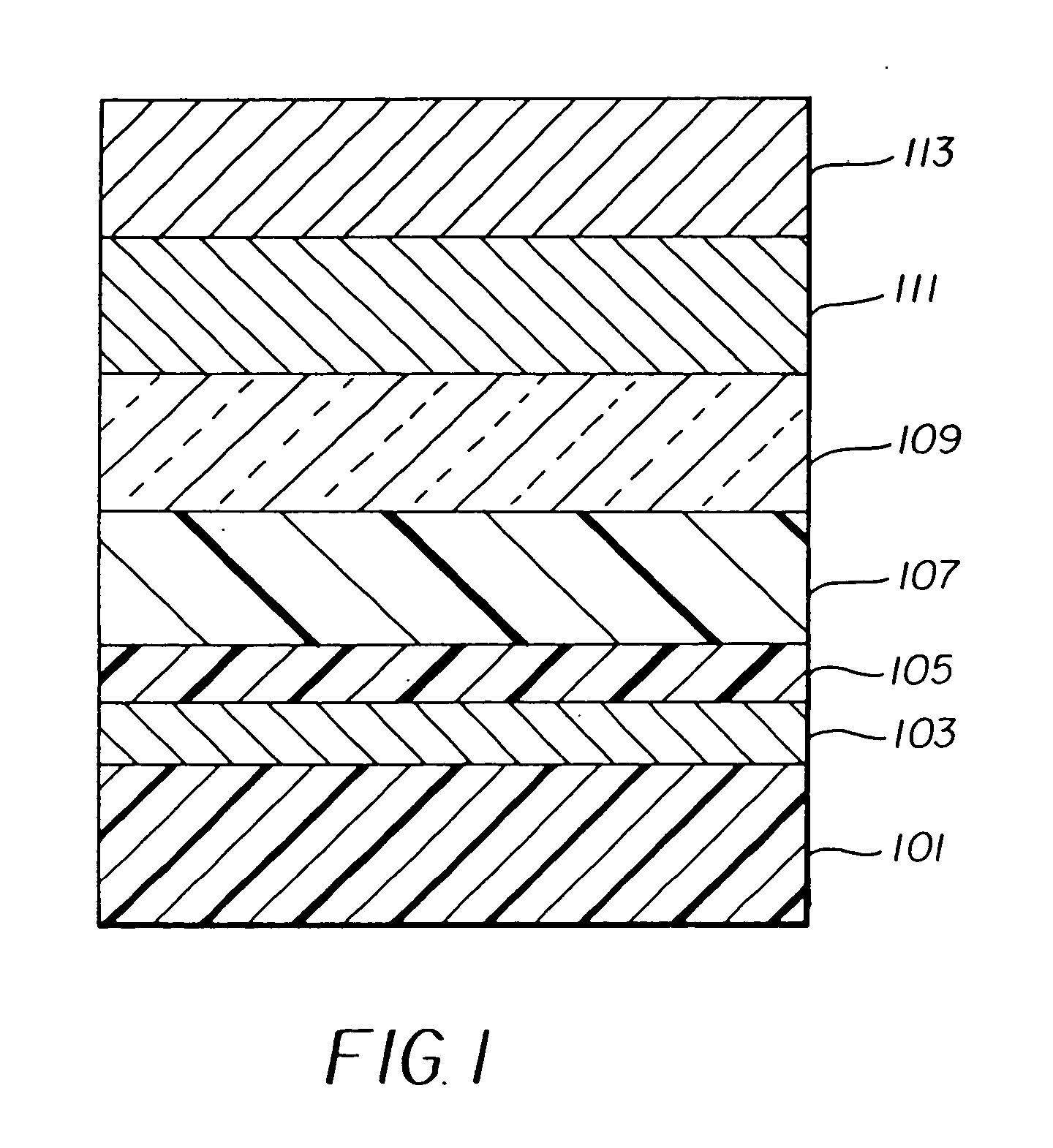
[0156] An EL device (Sample 1) satisfying the requirements of the invention was constructed in the following manner: [0157] 1. A glass substrate coated with an 85 nm layer of indium-tin oxide (ITO) as the anode was sequentially ultrasonicated in a commercial detergent, rinsed in deionized water, degreased in toluene vapor and exposed to oxygen plasma for about 1 min. [0158] 2. Over the ITO was deposited a 1 nm fluorocarbon (CFx) hole-injecting layer (HIL) by plasma-assisted deposition of CHF3. [0159] 3. A first hole-transporting layer (HTL)of Inv-1 having a thickness of 75 nm was then evaporated from a tantalum boat. [0160] 4. A 37.5 nm light-emitting layer (LEL) of tris(8-quinolinolato)aluminum(III) (AlQ3) and dopant DPQ (0.6 wt %, see structure below) were then deposited onto the hole-transporting layer. These materials were also evaporated from tantalum boats. [0161] 5. A 37.5 nm electron-transporting layer (ETL) of tris(8-quinolinolato)aluminum(II) (AlQ3) was the...


PUM

PropertyMeasurementUnit
thickaaaaaaaaaa
operating voltagesaaaaaaaaaa
thicknessaaaaaaaaaa

Abstract

An electroluminescent device comprises a layer containing a naphthalene compound represented by Formula (1),
wherein:
    • each R1 and R2 represents an independently selected substituent provided that adjacent substituents may join to form a ring; p and w independently are 0-3; the amine nitrogens on the naphthalene nucleus are located on separate rings; m and n independently are 0, 1 or 2;
    • each Arb represents an independently selected aromatic group; and each Ara represents an independently selected phenylene, biphenylene or naphthalene group;
    • provided that at least one R1 or R2 substituent of the naphthalene compound represented by Formula (1) is a sterically bulky substituent.

Description

FIELD OF INVENTION [0001] This invention relates to organic electroluminescent devices. More specifically, this invention relates to devices that emit light from a current-conducting organic layer and have high luminance and good stability. BACKGROUND OF THE INVENTION [0002] While organic electroluminescent (EL) devices have been known for over two decades, their performance limitations have represented a barrier to many desirable applications. In simplest form, an organic EL device is comprised of an anode for hole injection, a cathode for electron injection, and an organic medium sandwiched between these electrodes to support charge recombination that yields emission of light. These devices are also commonly referred to as organic light-emitting diodes, or OLEDs. Representative of earlier organic EL devices are Gurnee et al. U.S. Pat. No. 3,172,862, issued Mar. 9, 1965; Gurnee U.S. Pat. No. 3,173,050, issued Mar. 9, 1965; Dresner, “Double Injection Electroluminescence in Anthracen...

Claims


Application Information

Patent Timeline
Patent Type & Authority Applications(United States)
IPC IPC(8): C09K11/06H01L51/00H01L51/50H05B33/12H05B33/14
CPCC09K11/06H05B33/14C09K2211/1014C09K2211/1029C09K2211/1033C09K2211/1037C09K2211/1055C09K2211/107C09K2211/1088H01L51/0052H01L51/006H01L51/0081H01L51/5048H01L2251/308C09K2211/1011H10K85/633H10K85/615H10K85/324H10K50/14H10K2102/103
Inventor PARTON, RICHARD L.SLUSAREK, WOJCIECH K.OWCZARCZYK, ZBYSLAW R.TANG, CHING W.
Owner EASTMAN KODAK CO
Why Eureka
Try Eureka