[0007] Some degree of
anisotropy is necessary if an MTJ cell is to be capable of maintaining a magnetization direction and, thereby, to effectively store data even when write currents are zero. As cell sizes have continued to decrease, the technology has sought to provide a degree of
magnetic anisotropy by forming cells in a wide variety of shapes (eg. rectangles, diamonds, ellipses, etc.), so that the lack of inherent crystalline anisotropy is countered by a shape anisotropy. Yet this form of anisotropy brings with it its own problems. A particularly troublesome shape-related problem in MTJ devices results from non-uniform and uncontrollable edge-fields produced by shape anisotropy (a property of non-circular samples). As the
cell size decreases, these edge fields become relatively more important than the magnetization of the body of the cell and have an
adverse effect on the storage and reading of data. Although such shape anisotropies, when of sufficient magnitude, reduce the disadvantageous effects of super-
paramagnetism, they have the negative effect of requiring high currents to change the magnetization direction of the MTJ for the purpose of storing data.
[0008] Another way to address the problem that high currents are needed to change the magnetization direction of a free layer when the shape anisotropy is high, is to provide a mechanism for concentrating the fields produced by lower current values. This approach was taken by Durlam et al. (U.S. Pat. No. 6,211,090 B1) who teach the formation of a flux
concentrator, which is a soft magnetic (NiFe) layer formed around a
copper damascene current carrying line. The layer is formed around three sides of the
copper line which forms the digit line at the underside of the MRAM cell.
[0009] In conventional MRAM design, both the word and bit lines that intersect at the location of a particular MRAM cell must be carrying currents in order for that selected cell to be switched and for a 0 or a 1 to be written thereon. For the large number of other cells that lie along only the current carrying
bit line, or along only the current carrying word line, but not at their intersection, only the field of a
single line is experienced. Such cells are called half-selected. In an MRAM array, the half-selected cells must not be switched and the selected cell must be switched.
[0010] Every cell in an array can be thought of as being potentially under the influence of the superposition of two magnetic fields. Ideally, if only one line is carrying current, the
local field at the cell position should be insufficient to switch the cell and the cell can be said to be in the un-switched zone of the local
magnetic field. A problem arises, however, because variations in cell formation, particularly when cells are extremely small, can allow a cell to switch even when it is in the un-switched zone of the local magnetic field.
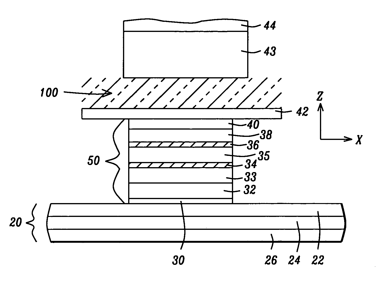
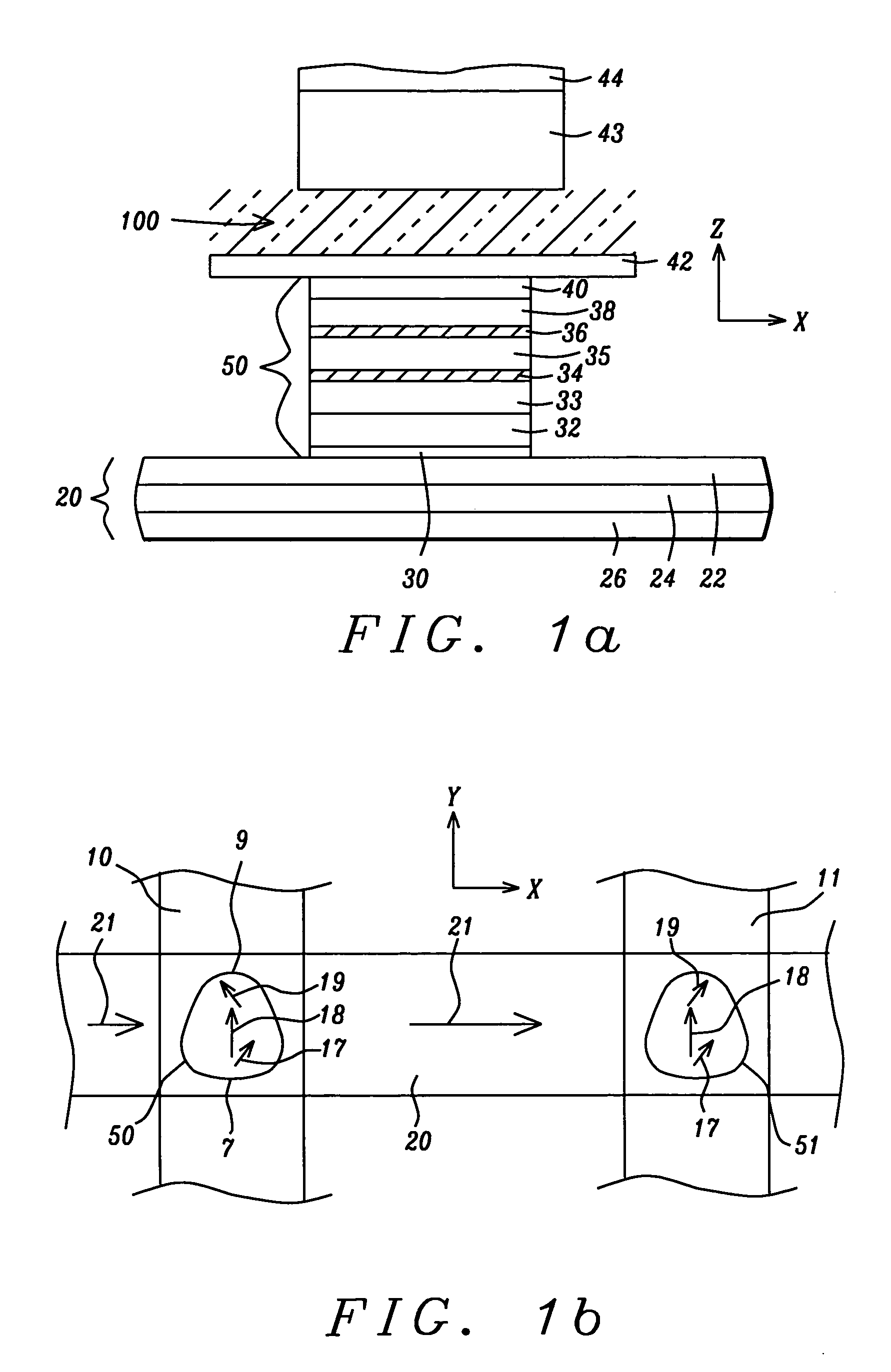
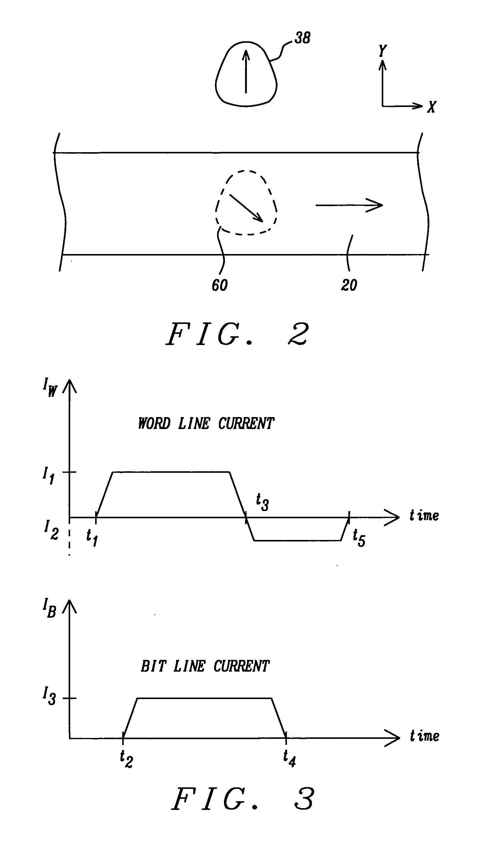
[0011] The purpose of the present invention is to create a
design margin for each cell, so that individual variations in
cell structure would be insufficient to place a non-selected cell within the switched zone of its local magnetic field. Such a
design margin can be achieved if the magnetization of a cell can be locked into a highly stable “C” state after each act of writing on the cell (holding it in a
stable state during write operations on other, nearby, cells), and if the cell can then be placed into a less stable “S” state when it is actually being written upon. In the method of the present invention, the capability of a free layer to be placed into C or S states is provided by magnetostatically
coupling it to a soft
magnetic layer (a cladding layer) formed around a bit line and by building in a small amount of magnetic anisotropy into the free layer. This additional magnetostatic interaction, along with the conventional magnetic fields produced by currents in the word and bit line, produces two states of flux closure within the free layer, which are the C and S states that are desired.
[0012] Cladding
layers surrounding current carrying write lines have been taught by others. Bloomquist et al. (U.S. Pat. No. 6,661,688 B2) teaches a write
line structure in which a cladding layer nearly completely surrounds a write line below a memory storage device. The cladding layer has an open space above the write line, so that it effectively forms two poles immediately adjacent to the storage device. The structure is said to provide a greater field at the storage device for a given current in the write line.

