Method for enhancing electrical characteristics of organic electronic devices

a technology of electrical characteristics and electronic devices, applied in the field of enhancement of can solve the problems of increasing manufacturing costs, unsatisfactory on-off, and impracticality of otfts, and achieve the effect of enhancing electrical characteristics of organic electronic devices

Inactive Publication Date: 2005-10-06
IND TECH RES INST
View PDF13 Cites 29 Cited by
  • Summary
  • Abstract
  • Description
  • Claims
  • Application Information

AI Technical Summary

Benefits of technology

[0008] The primary object of the invention is to provide a method for enhancing electrical characteristics

Problems solved by technology

Most of the prior methods for producing the organic semiconductor layer are at an experimental stage with unsatisfactory on-off ratio and use chloroform as the organic solvent which is a chemical forbidden by the industry.
In view of the above description, the conventional methods for producing organic TFT have at least the following disadvantages: (1) The OTFTs will be impractical if the on-off ratio is low.
(2) Although, th

Method used


Image

  • Method for enhancing electrical characteristics of organic electronic devices
  • Method for enhancing electrical characteristics of organic electronic devices
  • Method for enhancing electrical characteristics of organic electronic devices

Examples


Embodiment Construction

[0018] With the following descriptions and drawings, the objects, features, and advantages of the present invention can be better interpreted.

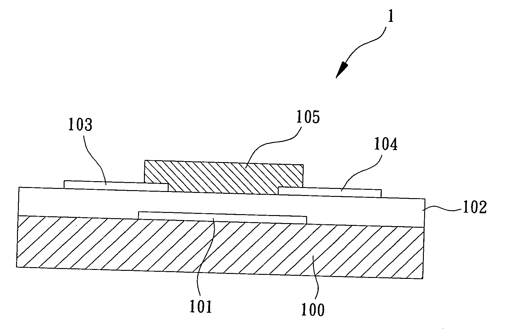
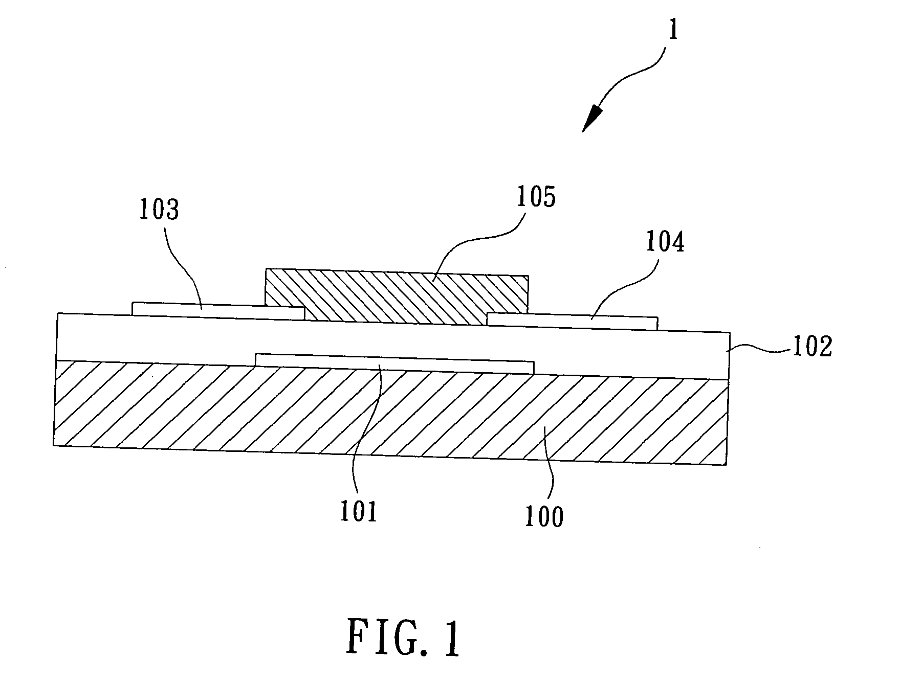
[0019] Please refer to FIG. 1, which is a schematic diagram of an organic thin-film transistor according to a preferred embodiment of the present invention. After a gate 101 is form on a substrate 100, an insulator layer 102 is formed using an organic insulator or an inorganic insulator with a source 103, a drain 104 and an organic semiconductor layer 105 further evaporated onto the insulator layer 102 between the source 103 and the drain 104 such that an organic thin-film transistor 1 is formed. A material selected from the group consisting of silicon wafer, glass substrate, metal substrate, plastic substrate, and so on, can be used as the substrate 100. A material selected from the group consisting of metal, organic conducting polymer and indium tin oxide (ITO), etc., can be used for the gate 101, the source 103 and the drain 104. The manuf...


PUM

PropertyMeasurementUnit
Ratioaaaaaaaaaa
Semiconductor propertiesaaaaaaaaaa
aaaaaaaaaa

Abstract

The present invention provides a method for enhancing electrical characteristics of organic electronic devices, especially for an organic thin-film transistors, comprising the steps of: providing a substrate with a gate and an insulator layer formed thereon; preparing an organic solution by mixing materials of an organic semiconductor polymer, an organic insulator polymer, a conducting particle and a solvent; forming an organic semiconductor layer on top of the insulator layer between the source and the drain using the organic solvent. Wherein, the organic semiconductor polymer can be a polymer selected from the group consisting of poly(3-alkylthiophene) (P3AT) with different alkyl side groups of 2, 4, 6, 8, 10, 12, and 18, as the P3HT is a P3AT with alkyl side group of 6, and the organic insulator polymer can be a polymer selected from the group consisting of poly(methylmethacrylate) (PMMA), and polybutylene terephthalate (PBT), etc. and the conducting particle can be a kind of particle selected from the group consisting of carbon nanotubes (CNTs), C60, and nano silver particle, and so on, and the solvent can be a solvent selected from the group consisting of xylene, toluene, and THF, and so forth.

Description

FIELD OF THE INVENTION [0001] The present invention relates to a method for enhancing electrical characteristics of organic electronic devices, and more particularly, to a method for enhancing electrical characteristics of organic thin-film transistors by improving the physical properties of the organic semiconductors. BACKGROUND OF THE INVENTION [0002] Organic semiconductors have been studied since the late 1940s, and the field effect thereof was first provided at 1970. However, not until 1987 that the organic field-effect transistor (OFET) was proven by Koezuka, et al. to be an electronic device with great potential. OFETs can be referred as the organic thin-film transistors (OTFT) for adopting the structure of thin-film transistors (TFTs). OTFTs provide two principle advantages over thin film transistors based on inorganic semiconductors—they can be fabricated at lower temperature and, potentially, at significantly lower cost. Moreover, Optimized OTFTs now show electronic charact...

Claims


Application Information

Patent Timeline
IPC IPC(8): H01L21/00H01L51/05H01L29/786H01L51/00H05B33/20
CPCB82Y10/00B82Y20/00B82Y30/00H01L51/0003H01L51/0036H01L51/0046H01L51/0545H01L2251/5369H10K71/12H10K85/113H10K85/211H10K10/466H10K2102/331
Inventor CHENG, HSIANG-YUANHO, JIA-CHONGHUANG, WEN-KUEI
Owner IND TECH RES INST
Why Eureka
Try Eureka