
Etching composition and method for etching a substrate

a technology of composition and substrate, which is applied in the direction of detergent composition, photomechanical apparatus, chemical apparatus and processes, etc., can solve the problems of difficult etching of limited possibilities of silicon oxide dielectrics used until now, and difficult to etch compounds such as hafnium oxide and hafnium silicate at a practical rate without attacking the easily damaged semiconductor material, etc., to achieve non-flammability

Inactive Publication Date: 2005-10-13
TOSOH CORP +1
View PDF7 Cites 8 Cited by
  • Summary
  • Abstract
  • Description
  • Claims
  • Application Information

AI Technical Summary

Benefits of technology

[0009] It is thus an object of the invention to provide etching compositions which can selectively etch poorly soluble hafnium compounds, particularly hafnium silicate and hafnium aluminate, and which are non-flammable.
[0012] By using the etching composition of the present invention, hafnium compounds can be selectively etched without damaging other semiconductor materials such as silicon oxide, and is safe to use industrially because it is non-flammable.
[0019] According to the method for etching a substrate of the present invention, hafnium compounds can be selectively etched without damaging other semiconductor materials such as silicon oxide.

Problems solved by technology

Scaling has also led to ever thinner dielectric films, but the limits of what is possible with the silicon oxide dielectrics used until now have been reached.
However, compounds such as hafnium oxide and hafnium silicate are not easy to etch, even with hydrofluoric acid.
Therefore, it has been very difficult to etch these dielectric films at a practical rate without attacking the easily damaged semiconductor material.
But this aqueous solution does not always have sufficient etchability for hafnium silicate and hafnium aluminate, in addition to which it causes considerable damage to other semiconductor materials (particularly, silicon oxide) nearby.
However, because this etchant is largely composed of the organic solvent and thus highly flammable, its use would require that semiconductor manufacturing equipment be given an explosion-proof construction, which is industrially undesirable.

Method used


Image

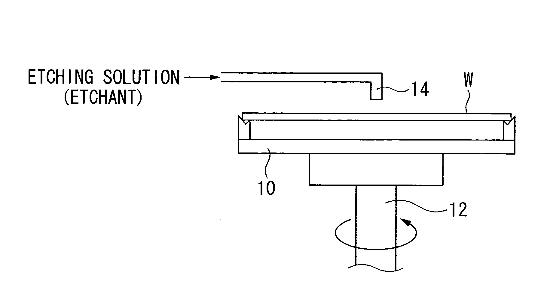
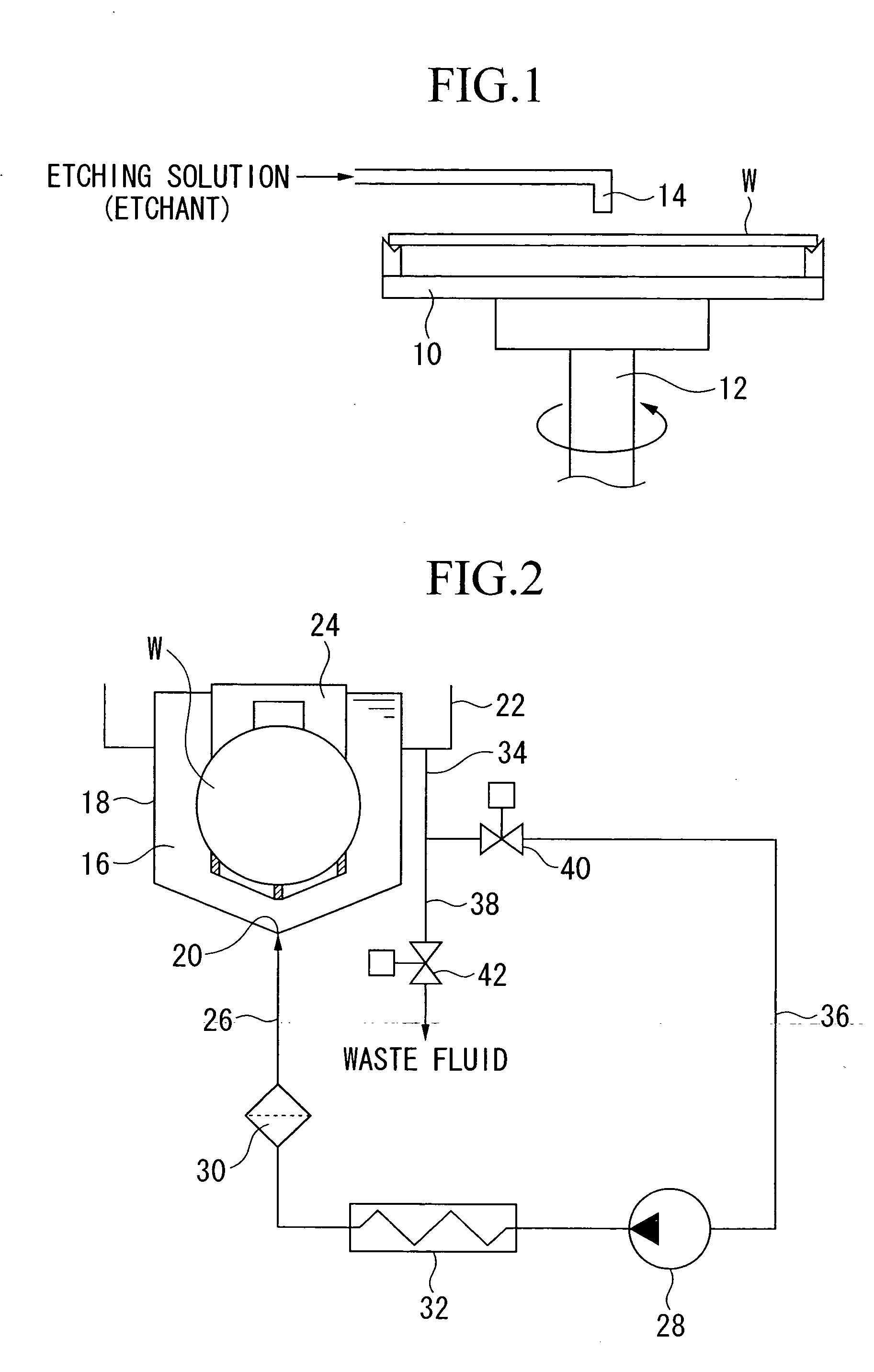
  • Etching composition and method for etching a substrate
  • Etching composition and method for etching a substrate

Examples


examples

[0054] Examples are given below to illustrate the invention, and are not intended to limit the scope of the invention. Here, for the sake of brevity, the following symbols are used below. [0055] SiF: silicon fluoride (which was produced by reacting silicic acid with hydrofluoric acid) [0056] AF: ammonium fluoride [0057] HCl: hydrochloric acid [0058] HF: hydrofluoric acid [0059] AC: ammonium chloride [0060] PA: phosphoric acid (orthophosphoric acid) [0061] IPA: 2-propanol [0062] HfSiOx: hafnium silicate [0063] HfSiONx: hafnium silicate nitride [0064] SiOx: silicon oxide [0065] SiN: silicon nitride

examples 1 to 15

, Comparative Examples 1 to 3

[0066] Silicon wafer substrates on which HfSiOx films or HfSiONx films were formed with film thicknesses of 10 nm by a CVD (chemical vapor deposition) method, silicon substrates on which thermal oxide films (SiOx) were formed with film thicknesses of 300 nm, and silicon substrates on which SiN films were formed with film thicknesses of 100 nm were prepared. Etching compositions shown in Table 1 were also prepared, and each was added to its own polyethylene vessel. In the etchant compositions shown in Table 1, the balance of the composition was water.

TABLE 1Etchant composition (wt. %)FluorideChlorideTemperatureRate of etching (nm / min)compoundcompoundAdditive(° C.)HfSiOxHfSiONxSiOxSiNExample 1AF (0.1)HCl (10)801.0961.0340.120Example 2AF (0.1)HCl (10)400.6740.8800.172Example 3AF (0.1)HCl (10)250.3840.5140.122Example 4AF (0.1)AC (10)PA (10)800.9501.0700.188Example 5AF (0.1)AC (10)PA (10)600.6060.7780.000Example 6AF (0.1)AC (10)PA (10)500.5100.6020.010Examp...


PUM


Abstract

This etching composition for etching hafnium compound, includes a fluoride compound and a chloride compound. This method for etching a substrate, includes etching a film which contains hafnium compound and is formed on a substrate by using an etching composition, wherein the etching composition contains a fluoride compound and a chloride compound.

Description

BACKGROUND OF THE INVENTION [0001] 1. Field of the Invention [0002] The present invention relates to compositions for etching hafnium compounds such as hafnium silicate and hafnium aluminate. More specifically, the invention relates to compositions for etching dielectric films which contain hafnium silicate or hafnium aluminate and are used in semiconductor devices. [0003] This application claims priority from Japanese Patent Application No. 2004-087225, filed on Mar. 24, 2004, the disclosure of which is incorporated herein by reference. [0004] 2. Background Art [0005] With the rapid advances made over the past few years in information technology, there exists today a trend toward higher speed operation in large-scale integration (LSI, ULSI, VLSI) chips through smaller circuit geometries (scaling), higher packing density, and increased levels of integration. The use of new materials in semiconductor circuits is being studied for this purpose. Scaling has also led to ever thinner die...

Claims


Application Information

Patent Timeline
IPC IPC(8): C09K13/08G03F7/004H01L21/00H01L21/311H01L21/44
CPCH01L21/67086H01L21/31111C09K13/08H01L21/30604C11D2111/22
Inventor IIARA, YASUSHITAKAHASHI, FUMIHARUHAYASHI, HIROAKI
Owner TOSOH CORP
Learn More