Method of fabricating semiconductor by nitrogen doping of silicon film

a technology of amorphous silicon and nitrogen doping, which is applied in the direction of coating, chemical vapor deposition coating, metallic material coating process, etc., can solve the problems of insufficient breakdown voltage, high breakdown voltage, and many defects in pure amorphous silicon, so as to reduce the breakdown voltage, reduce the conductivity, and reduce the effect of amorphous silicon conten

Inactive Publication Date: 2005-10-20
PAN JIT AMERICAS
View PDF6 Cites 60 Cited by
  • Summary
  • Abstract
  • Description
  • Claims
  • Application Information

AI Technical Summary

Benefits of technology

[0015] An advantage of the present invention is that the nitrogen-doping of the deposited amorphous silicon film has reduced conductivity and a higher breakdown voltage, electrical properties that are desirable fo...

Problems solved by technology

For fabrication of semiconductors, however, pure amorphous silicon has been found to contain too many defects (i.e., too many dangling bonds).
One of the shortcomings of semiconductor films made of deposited amor...

Method used


Image

  • Method of fabricating semiconductor by nitrogen doping of silicon film
  • Method of fabricating semiconductor by nitrogen doping of silicon film
  • Method of fabricating semiconductor by nitrogen doping of silicon film

Examples


Embodiment Construction

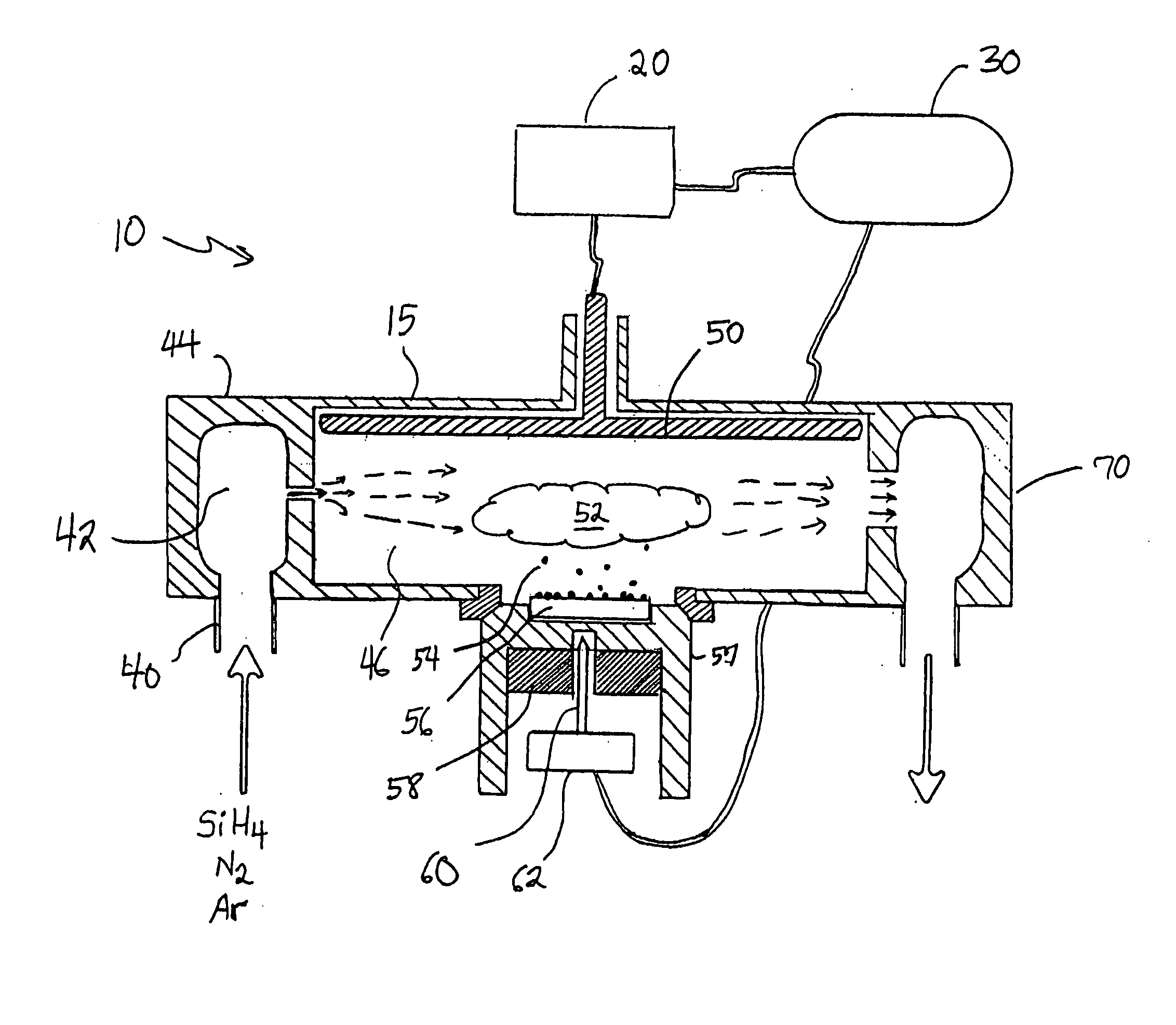
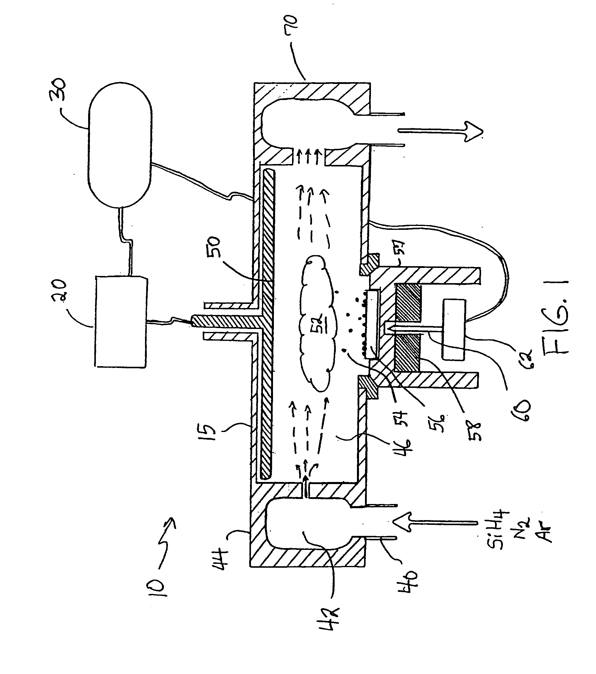
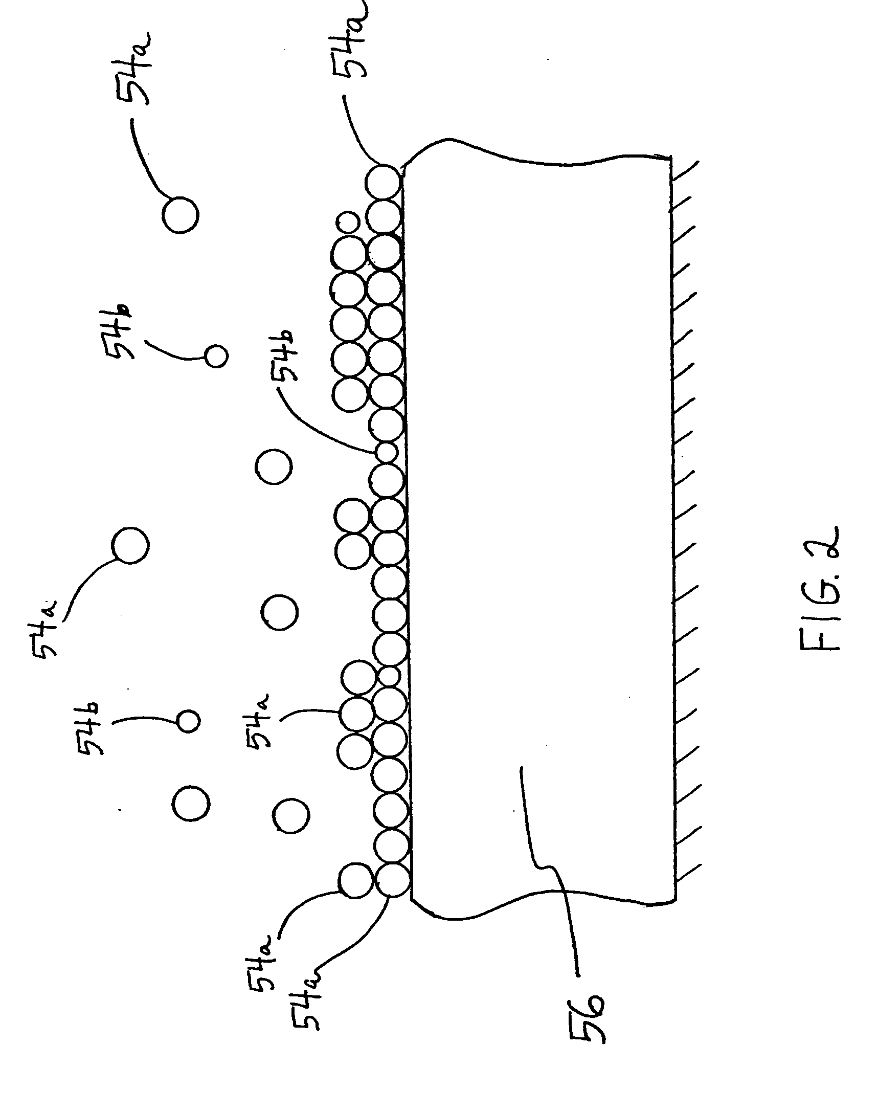
[0028]FIG. 1 illustrates schematically a plasma-enhanced chemical vapor deposition (PECVD) process whereby amorphous silicon is doped with nitrogen and deposited as a film on a substrate or carrier such as an ASIC wafer. The PECVD process shown in FIG. 1 uses a PECVD reactor system, such as the (Advanced Semiconductor Materials “ASM”) ASM Plasma III System, which is designated generally by the reference numeral 10.

[0029] The PECVD reactor system 10 has a reactor 15, a power source 20 for generating radio-frequency power in the reactor and a control unit 30 for controlling various reaction parameters, as will be elaborated below. The reactor has a gas manifold 40 for the intake of precursors or reagents. The precursors are silane, or SiH4, (as the source of silicon), N2 for nitrogen doping, and an inert gas such as Argon to facilitate ionization. The precursors enter a gas reservoir 42 in an injector head 44. The injector head 44 injects the precursor gases into a reaction chamber 4...


PUM

PropertyMeasurementUnit
Poweraaaaaaaaaa
Poweraaaaaaaaaa
Poweraaaaaaaaaa

Abstract

A method of fabricating a semiconductor uses chemical vapor deposition, or plasma-enhanced chemical vapor deposition, to deposit an amorphous silicon film on an exposed surface of a substrate, such as ASIC wafer. The amorphous silicon film is doped with nitrogen to reduce the conductivity of the film and/or to augment the breakdown voltage of the film. Nitrogen gas, N2, is activated or ionized in a reactor before it is deposited on the substrate.

Description

TECHNICAL FIELD [0001] The present invention relates, in general, to the manufacturing of semiconductors with deposited silicon films, and, in particular, to the doping of an amorphous silicon film to achieve desired electrical properties in the film. BACKGROUND OF THE INVENTION [0002] Chemical vapor deposition and plasma-enhanced chemical vapor deposition are processes that are widely used to fabricate semiconductor devices. [0003] Chemical vapor deposition (CVD) is a chemical reaction in which gaseous molecules called precursors are transformed into a thin film on the surface of a substrate, such as an application-specific integrated circuit (ASIC) wafer. [0004] Plasma-enhanced chemical vapor deposition (PECVD) is a similar process which occurs in a reactor wherein a strong electric field causes decomposition of a gaseous compound into a plasma (of highly ionized gases). This reaction leads to precipitation of a film onto the substrate surface. [0005] CVD and PECVD processes for t...

Claims


Application Information

Patent Timeline
IPC IPC(8): C23C16/24C23C16/34H01L21/205H01L21/365
CPCC23C16/24C23C16/345H01L21/0262H01L21/02576H01L21/02532
Inventor KOUNTZ, MICHAELENGLE, GEORGEEVERS, STEVEN
Owner PAN JIT AMERICAS
Why Eureka
Try Eureka