Controlling the properties and uniformity of a silicon nitride film by controlling the film forming precursors
- Summary
- Abstract
- Description
- Claims
- Application Information
AI Technical Summary
Benefits of technology
Problems solved by technology
Method used
Image

Examples
example one
The Overall Process For Forming a TFT
[0054] To provide a general understanding of the relationship of the PECVD deposited a-SiNx:H gate dielectric film and the a-SiNx:H passivation dielectric film relative to the other components of the TFT, a brief description of the overall fabrication process of the TFT embodiment shown in FIG. 1 is presented below.
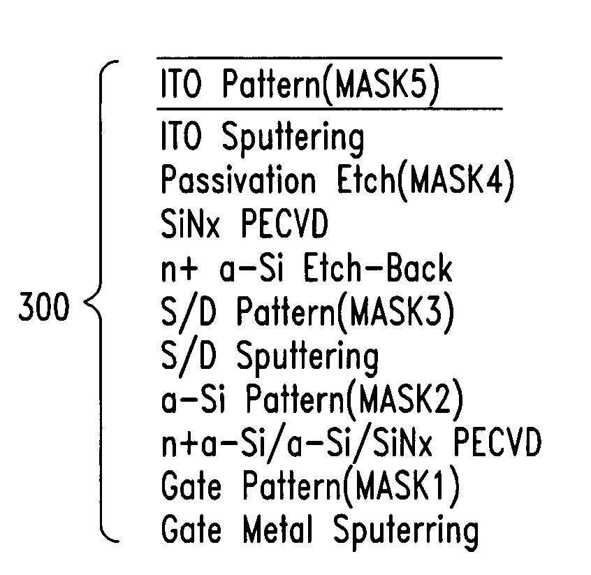
[0055]FIG. 3 show a series of process steps 300 which may be carried out to create the TFT device shown in FIG. 1. FIG. 3 also provides a schematic top-view 336 of a substrate including several TFT structures.
[0056] In the first step, “Gate Metal Sputtering”, a conductive layer 302 is sputter deposited over a glass substrate 301 using techniques known in the art. In this particular instance the substrate 301 is a glass substrate having a thickness of 0.7 mm. The conductive layer 302 is actually a bilayer, where the bottom portion of the layer is a chrome layer, with an overlying layer of an aluminum neodymium alloy.
[0057] In the se...
example two
The Process For Depositing an a-SiNx:H Gate Dielectric Layer
[0067] We have previously described all of the performance requirements for the a-SiNx:H gate dielectric layer. We carried out extensive experimentation in an effort to produce a PECVD deposited a-SiNx:H gate dielectric layer which met the performance requirements and which provided a uniformity in film thickness and uniformity in film properties, including structural and chemical composition, when PECVD deposited over a large surface area, larger than 1000 mm×1000 mm, for example. One basic requirement is that the a-SiNx:H film deposition rate is more than 1000 Å / min and typically more than 1300 Å / min, so that the fabrication throughput for the TFT provides adequate productivity to be economically competitive. The basic requirements for the a-SiNx:H film are that: the Si—H bonded content of the a-SiNx:H film is less than about 15 atomic %; the film stress ranges from about 0 to about −1010 dynes / cm2; the refractive index ...
PUM
| Property | Measurement | Unit |
|---|---|---|
| Temperature | aaaaa | aaaaa |
| Temperature | aaaaa | aaaaa |
| Temperature | aaaaa | aaaaa |
Abstract
Description
Claims
Application Information
 - Generate Ideas
- Intellectual Property
- Life Sciences
- Materials
- Tech Scout
- Unparalleled Data Quality
- Higher Quality Content
- 60% Fewer Hallucinations
Browse by: Latest US Patents, China's latest patents, Technical Efficacy Thesaurus, Application Domain, Technology Topic, Popular Technical Reports.
© 2025 PatSnap. All rights reserved.Legal|Privacy policy|Modern Slavery Act Transparency Statement|Sitemap|About US| Contact US: help@patsnap.com