Printed circuit board and method for processing printed circuit board

a printed circuit board and printed circuit board technology, applied in the direction of dielectric characteristics, light absorption dielectrics, etching metal masks, etc., can solve the problems of increasing the production cost difficult to advance the packaging density of printed circuit boards, and inability to process copper foil sheets, etc., to achieve improved processing efficiency, reduce processing process, and improve the effect of hole quality

Inactive Publication Date: 2005-11-03
HITACHI SEIKO LTD
View PDF4 Cites 10 Cited by
  • Summary
  • Abstract
  • Description
  • Claims
  • Application Information

AI Technical Summary

Benefits of technology

[0010] An object of the invention is to provide a printed circuit board in which advance of packaging density of the printed circuit board and reduction in production cost can be attained while processing quality can be made uniform, a method for processing the printed circuit board.
[0020] Because an electric conductor layer can be processed by laser light, especially CO2 laser light, the processing process can be reduced while the processing efficiency can be improved. In addition, because a hole shape suitable to the plating process can be obtained, the quality of the hole can be improved.

Problems solved by technology

In the case of CO2 laser light, if energy is low, it is impossible to process the sheets of copper foil because large part of the applied laser light is reflected on surfaces of the sheets of copper foil.
In the case of the technique described in JP-A-2002-118344, the production cost of a printed circuit board increases if a window needs to be provided accurately, and it is difficult to advance the packaging density of the printed circuit board if the window needs to be enlarged.
However, because excessive energy is supplied to an electrically insulating layer under the hole at the same time that the hole is formed in the copper foil, the electrically insulating layer just under the hole is gouged out so largely that the overhang length of copper becomes large.
In such a case, the plating thickness of the corner in the bottom of the hole may become thin because the plating is concentrated in the inlet of the hole, or a void may be generated in the inside of the hole because the inlet is blocked with the plating.
Accordingly, there is a problem not only in deterioration of external appearance but also in a pattern-forming process as an after-process.

Method used


Image

  • Printed circuit board and method for processing printed circuit board
  • Printed circuit board and method for processing printed circuit board
  • Printed circuit board and method for processing printed circuit board

Examples


embodiment 1

[0030] Processing of a first layer of copper foil disposed in a printed circuit board will be described first. Incidentally, as will be described later, a subject of the invention is a printed circuit board which is provided as a material applied to a process of producing a completed printed circuit board.

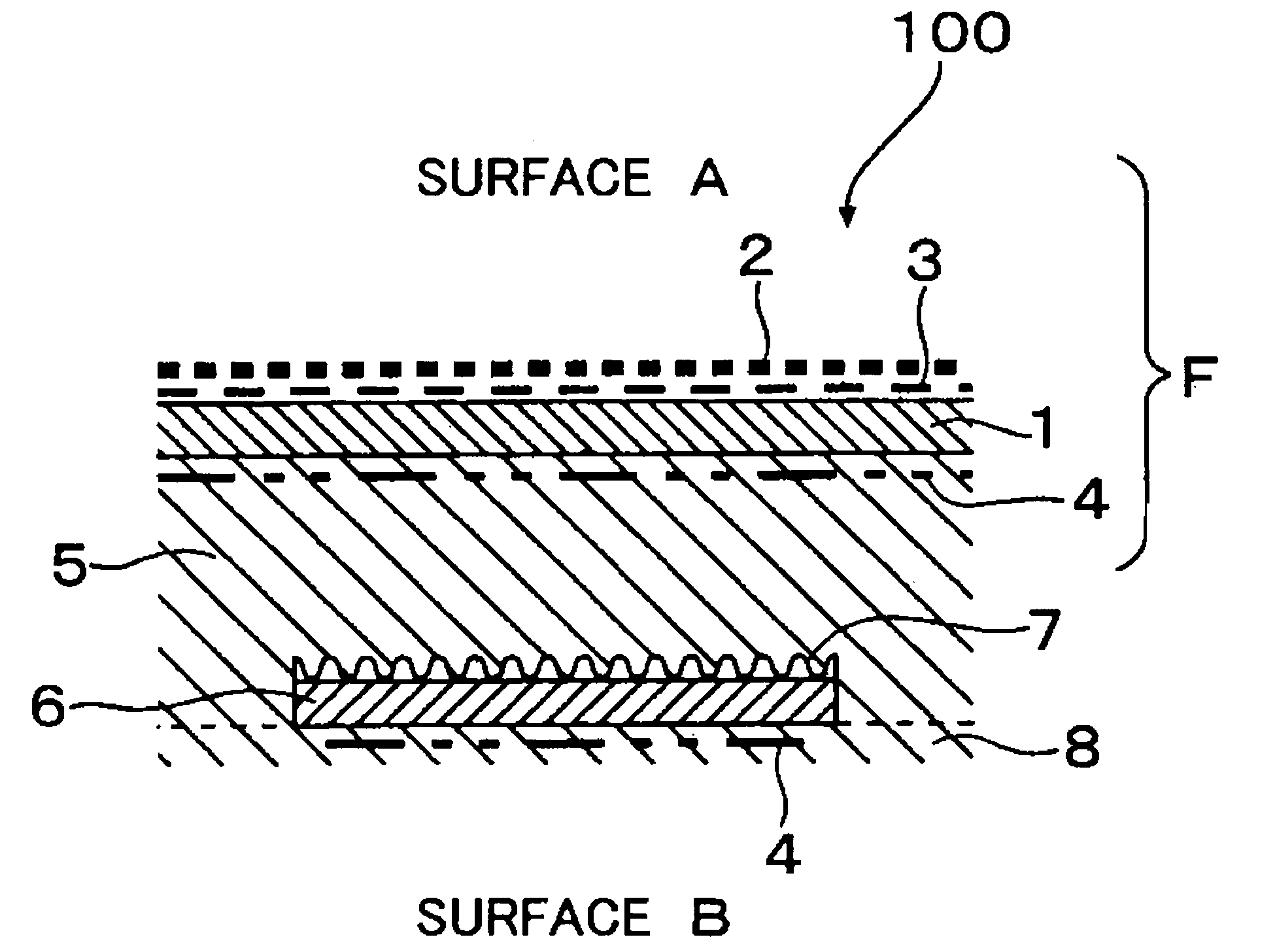
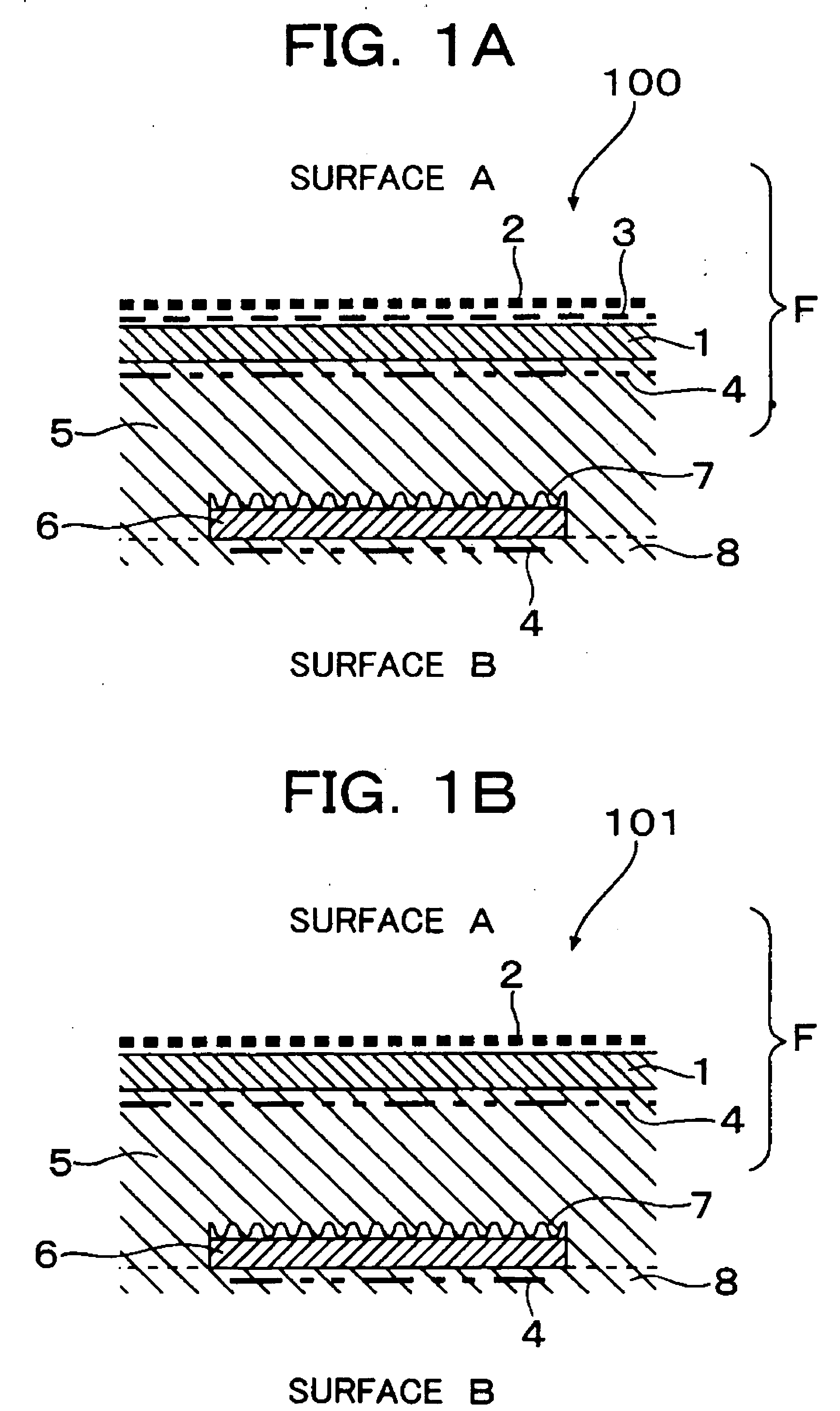
[0031]FIG. 1A is a sectional view typically showing a first printed circuit board 100 according to the invention.

[0032] In the printed circuit board according to the invention, the thickness of a sheet of copper foil 1 which is an electric conductor layer provided as a first layer (hereinafter referred to as “first layer”) is from 5 μm to 18 μm. A CU2O layer 3 containing CU2O (cuprous oxide) as a main component as represented by the thick broken line is formed in a portion of a surface (surface A side) abutting on copper. A CuO layer 2 containing CuO (cupric oxide) as a main component as represented by the thin broken line is formed on an upper side (surface A side) of the CU2O l...

embodiment 2

[0070] Next, processing of inner layers (the second layer, the electric conductor layer in the second layer, etc.) disposed in the printed circuit board will be described.

[0071]FIGS. 4A to 4D show an example in which the first and second layers ate connected to each other according to the invention. Conductor layers F and S are disposed as the first and second layers respectively. Fiducial marks (alignment marks) 18 are formed at the same time that circuits in the second layer are formed.

[0072] Next, a procedure of processing will be described.

[0073] (1) One of the fiducial marks 18 is exposed from the state shown in FIG. 4A. In this case, a beam (Bt) having a top hat type energy distribution is rotated around the center axis of the fiducial mark 18 while the radius of the beam is changed as shown in FIG. 4B. In this manner, the first layer (conductor layer F) is processed by a spot facing treatment. On this occasion, the intensity of the beam can be increased to a certain degree...

embodiment 3

[0079] Next, a procedure of processing the blind hole for connecting the first, second and third layers disposed in the printed circuit board will be described.

[0080]FIGS. 5A to 5D show an example in which the first to third layers are connected to one another according to the invention.

[0081] (1) One of the fiducial marks 18 is exposed from the state shown in FIG. 5A. In this case, a beam (Bt) having a top hat type energy distribution is rotated around the center axis of the fiducial mark 18 while the radius of the beam is changed. In this manner, the first layer (conductor layer F) is processed by a spot facing treatment. On this occasion, it is necessary to consider that the sheet of copper foil T is prevented from being damaged because the second layer is the sheet of copper foil T (FIG. 5B).

[0082] (2) A hole is formed in a desired position of the first layer with reference to the exposed fiducial mark 18.

[0083] In this embodiment, a hole having a diameter of 150 to 200 μm i...


PUM

PropertyMeasurementUnit
thicknessaaaaaaaaaa
surface roughnessaaaaaaaaaa
reflectivityaaaaaaaaaa

Abstract

The invention is to provide a printed circuit board in which advance of packaging density of the printed circuit board and reduction in production cost can be attained while processing quality can be made uniform, a method for processing the printed circuit board and a method for producing the printed circuit board. There is provided a printed circuit board including an alternate laminate of electric conductor layers and electrically insulating layers, wherein a coating layer capable of absorbing laser light but insoluble in an etching solution dissolving the electric conductor layers is provided on a front surface of a first one of the electric conductor layers. In this case, the coating layer may be provided on a front surface of a rear one of the electric conductor layers. Each of the electric conductor layers may contain Cu as a main component while the coating layer may contain CuO as a main component. The coating layer may have a thickness not thinner than 0.6 μm.

Description

FIELD OF THE INVENTION [0001] The present invention relates to a printed circuit board and a method for processing the printed circuit board. BACKGROUND ART [0002] In a multilayer printed circuit board, blind holes or through-holes for connecting sheets of copper foil to one another are formed in order to electrically connect sheets of copper foil (electric conductors) disposed in respective layers. The blind holes or through-holes formed thus are plated to thereby electrically connect the sheets of foil. [0003] In the case of CO2 laser light, if energy is low, it is impossible to process the sheets of copper foil because large part of the applied laser light is reflected on surfaces of the sheets of copper foil. Therefore, for example, for formation of a blind hole for connecting a first layer (copper foil on a front surface) and a second layer (copper foil disposed under the first layer with an electrical insulator interposed therebetween), a hole (window) is formed in the first l...

Claims


Application Information

Patent Timeline
Patent Type & Authority Applications(United States)
IPC IPC(8): B32B3/00H05K1/02H05K3/00H05K3/06H05K3/42H05K3/46
CPCH05K1/0269Y10T428/24917H05K3/0035H05K3/0038H05K3/06H05K3/062H05K3/421H05K3/427H05K3/429H05K3/4652H05K3/4679H05K2201/0112H05K2201/09845H05K2201/09918H05K2203/0315H05K2203/0346H05K2203/0554H05K3/0008H05K3/46
Inventor ARAI, KUNIOAKAHOSHI, HARUO
Owner HITACHI SEIKO LTD
Why Eureka
Try Eureka