

Semiconductor device and its manufacturing method
a technology of semiconductors and semiconductors, applied in semiconductor devices, electrical equipment, transistors, etc., can solve the problems of dielectric breakdown field strength, high blocking voltage voltage power devices, and silicon carbide substrate-based mosfets with about one-tenth the channel mobility of silicon substrate-based mosfets
- Summary
- Abstract
- Description
- Claims
- Application Information
AI Technical Summary
Benefits of technology
Problems solved by technology
Method used
Image

Examples
Embodiment Construction
[0071] The present invention provides a semiconductor device and method of manufacturing same, in which the focus is on a technology for forming an oxide layer / silicon carbide interface in the (000-1) face, which has higher dielectric breakdown field strength than the (11-20) face and higher channel mobility than the (0001) face. The embodiments of the present invention will now be described in detail with reference to the drawings.
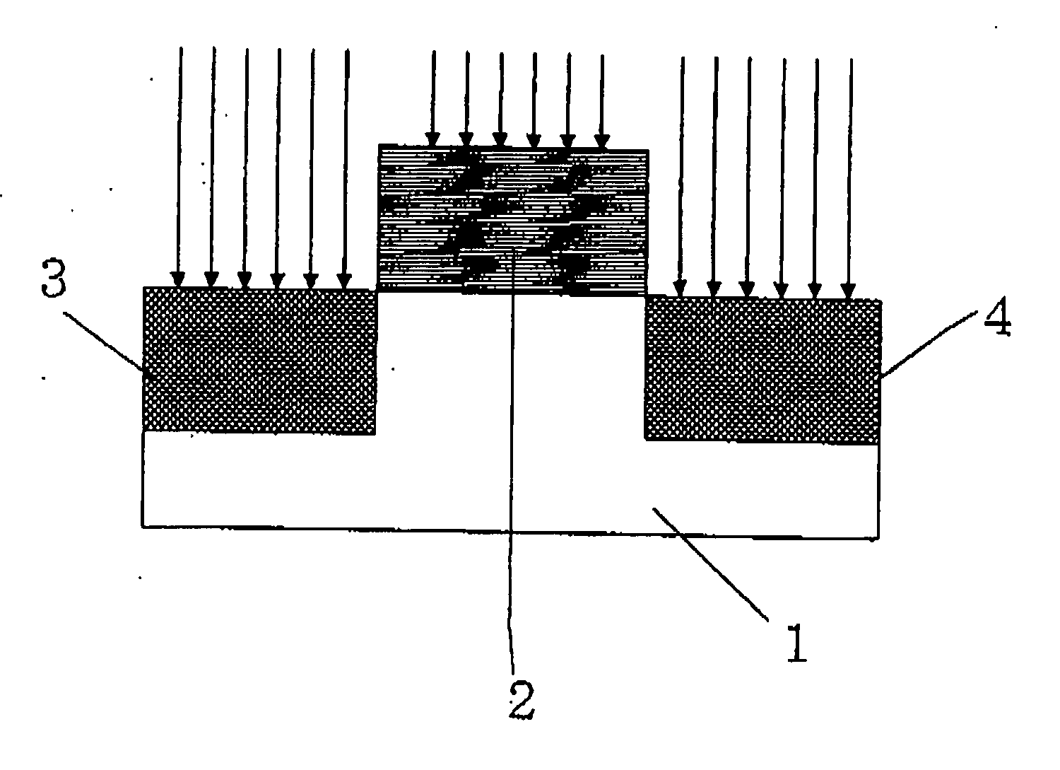
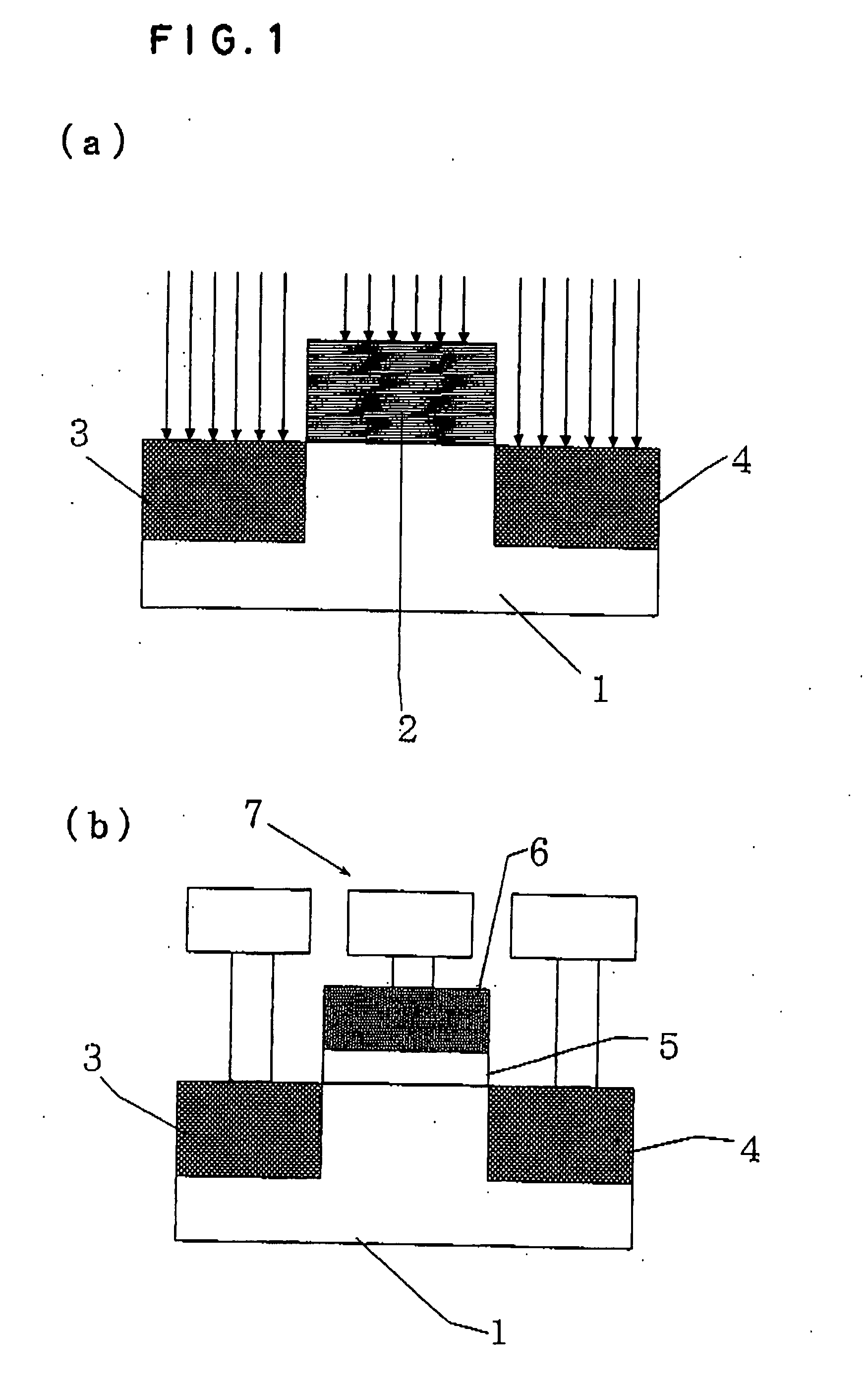
[0072] A specific example of the method of manufacturing a semiconductor device will be described with reference to FIG. 1.
[0073]FIG. 1 is a cross-sectional view of the process of fabricating a MOS transistor using a silicon carbide substrate, shown partway through the fabrication procedure. FIG. 1(a) shows a (000-1)-faced p-type silicon carbide substrate 1 (4H-SiC, impurity concentration of 5×1015 cm−3) on which RIE (reactive ion etching) has been used to form photolithography alignment marks, following standard RCA cleaning. It is also possible to use...
PUM
| Property | Measurement | Unit |
|---|---|---|
| temperature | aaaaa | aaaaa |
| temperature | aaaaa | aaaaa |
| temperature | aaaaa | aaaaa |
Abstract
Description
Claims
Application Information