Electric signal connecting device and probe assembly and probing device using the same

a technology of connecting device and probe, which is applied in the direction of individual semiconductor device testing, semiconductor/solid-state device testing/measurement, instruments, etc., can solve the problems of falling measurement yield, difficulty in controlling contact pressure to a constant level, and difficulty in satisfying the area occupied by circuit terminals and wiring widths, so as to simplify the drawing of wiring and the connection terminal structure

Inactive Publication Date: 2005-11-17
KIMOTO GUNSEI
View PDF21 Cites 25 Cited by
  • Summary
  • Abstract
  • Description
  • Claims
  • Application Information

AI Technical Summary

Benefits of technology

[0037] As a result, it has become possible to contain the sliding of the whole multiple array structure due to thermal expansion, and it has become easily possible to conduct probing tests by bringing the vertical probes arranged at each crossing position of the units in the X direction and the units in the Y direction into contact en bloc with all the pads of the semiconductor chips to be tested formed on a semiconductor wafer without any displacement in position. It is also possible to use the probing device of the present invention in a burn-in test wherein electric stresses are applied to circuits in a high temperature to conduct acceleration tests of semiconductor chips. The use of ribbon-shaped resin films simplifies the drawing of wiring and the connecting terminal structure to outside devices, and consequently it becomes possible to provide probing devices solving the thermal expansion problem and the signal wiring problem.

Problems solved by technology

In particular, an issue arising out of the miniaturization of pad arrangement (narrowing of pitch) is that the structure of probe for obtaining electric conductivity by bringing it into contact with the pads of semiconductor chips at the time of electric property tests or circuit test of electronic devices must be matched to the miniaturization of pad arrangement, and various measuring means are used to cope with this progress in miniaturization of pad arrangement.
However, this cantilever structure had a problem of damaging the pads due to shifts in the horizontal direction of the tip that serve as the contact point when it comes into contact with the pad, or resulting in a fall in the measurement yield due to the tip falling off the pad.
In addition, there were problems in that only a tip could be measured at a time and that the precision of fixing each probe varied resulting in a difficulty of controlling the contact pressure to a constant level.
However, the miniaturization of circuit patterns on a probe card which is a printed wire board is limited by fabrication technology, and therefore, it is difficult for the area occupied by circuit terminals and wiring width to satisfy the requirements matching the pad pitch, and also because of a limit to the pitch interval for soldering, it was impossible to vertically fix a vertical probe to the probe card according to the pad pitch of the semiconductor chip as miniaturization progressed.
Thus, in a probe card the proportion of its plane area being occupied by the area of circuit terminals and the width of circuit interconnection is important and obstructs the narrowing of pitch of circuit terminals.
However, due to a large area represented by these through-holes, the presence of through-holes was an obstacle for narrowing the pitch of arranging circuit terminals.
Thus, any attempt to fix vertical probes to a probe card was plagued by the difficulty of narrowing the pitch of circuit terminals and required an advanced technology in soldering and a large number of manual operations leading to high costs of manufacturing.
Nevertheless, this probing device is not different from others in that a plurality of semiconductor chips formed on a semiconductor wafer are tested successively one after another, and it is necessary to move the wafer stage by one tip for each test.
However, in the case of a wafer on which 200 chips each having 100 pads are formed for example, 100×200=20,000 signal wiring cables will be required for each multiple array vertical probe assembly, and it is difficult to efficiently draw such a number of signal wiring cables from a multiple array vertical probe assembly and connect them to outside testing apparatuses.
In particular, as the position of vertical probes moves closer to the perimeter of the wafer, the discrepancy of pitch of vertical probes will be cumulated, grow larger and it will become impossible to probe.
While the pitch provided by a flat cable is narrow 30 μm pitch, an important issue is how to cope with the wiring of test circuits in view of such narrow pitch contacts.
Such a force is likely to create a problem of deformation of mechanical parts.

Method used


Image

  • Electric signal connecting device and probe assembly and probing device using the same
  • Electric signal connecting device and probe assembly and probing device using the same
  • Electric signal connecting device and probe assembly and probing device using the same

Examples


embodiment 1

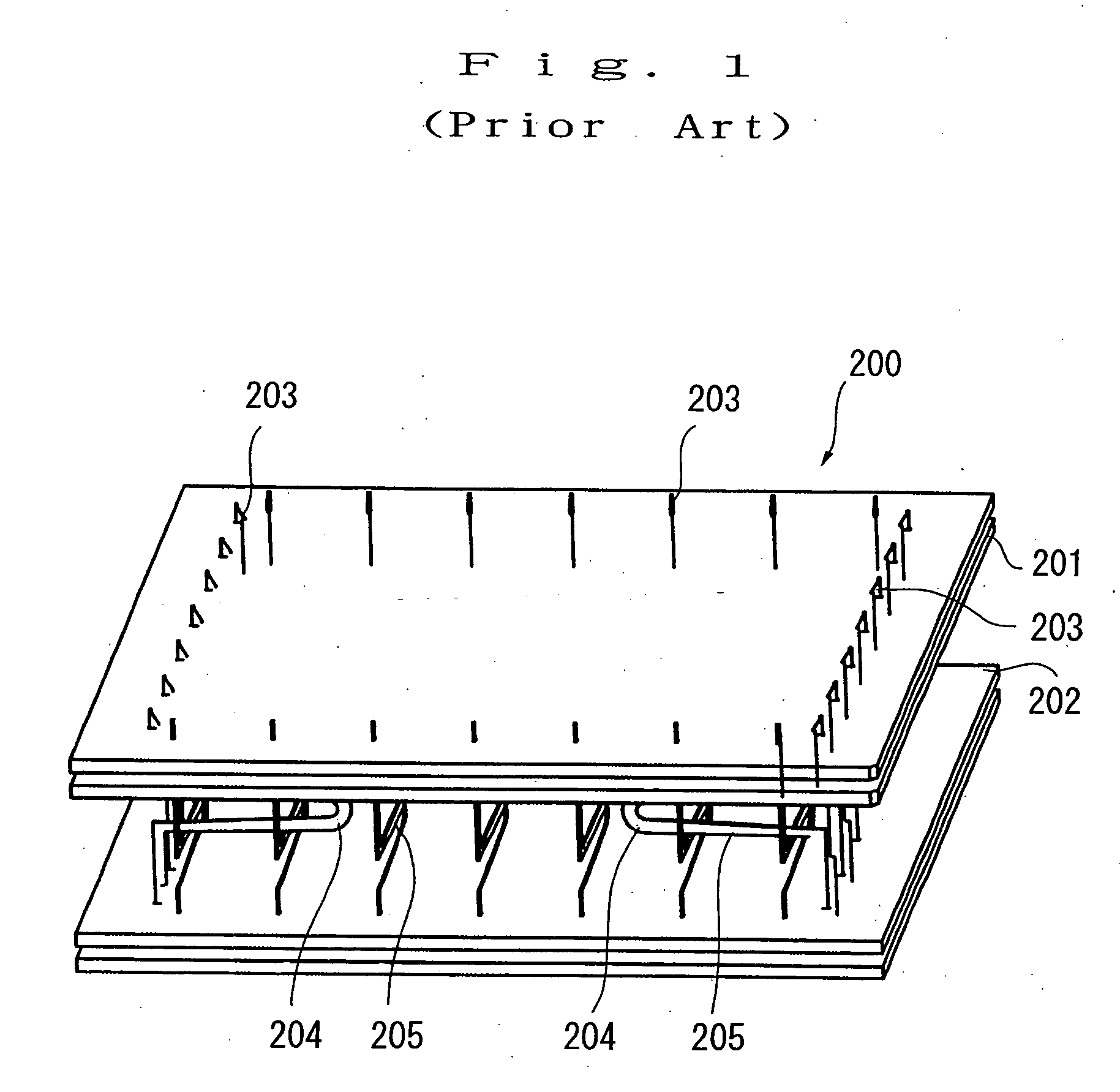
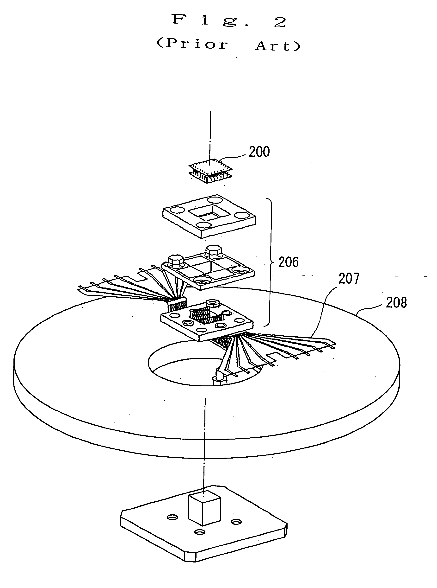
[0099] The following is a detailed description of Embodiment 1 of the probing device of the present invention with reference to drawings. The present embodiment 1 is an effective system when it is applied to the current system shown in FIG. 3, and the integration of wiring lines with probes eliminates the necessity of expensive multilayered board and the like of the prior probe card.

[0100]FIG. 5 is a perspective view showing Embodiment 1 of a multiple array vertical probe assembly according to the present invention. The basic structure of the multiple array vertical probe assembly according to the present Embodiment 1 is made up by combining in the grid form a unit in the X direction 5 formed by arranging in the vertical direction a plurality of ribbon-shaped films in the X direction 1 on which a plurality of vertical probes 3 patterned by etching in the longitudinal direction, and, like this unit in the X direction 5, a unit in the Y direction 6 formed by arranging in the vertical...

embodiment 2

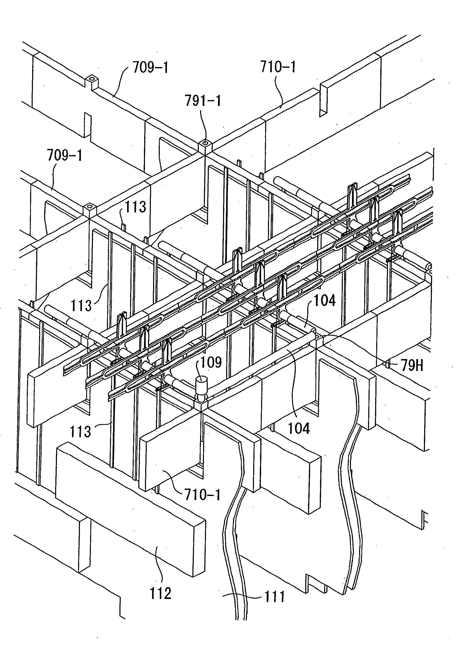
[0110]FIG. 6 is a partial perspective view describing the structure of the probing device according to Embodiment 2 of the present invention. Embodiment 2 of the present invention is characterized in that the acting point of contact pressure and the supporting parts subjected to this contact pressure are in the ending position of the curved parts regardless of the number of arrays of multiple arrays and the number of wiring lines, and a good spring characteristic of probes can be obtained. It is also characterized in that the wiring part is behind the supporting part and is unlikely to be affected by the resiliency property of probes, a sufficient space available for electric wiring can be secured, and wiring pattern forms sufficiently taking into account electric property can be obtained. And the probing device using the multiple array vertical probe assembly of the present Embodiment 2 is not constituted by arranging individual probe assemblies in the matrix pattern as in the past...

embodiment 3

[0132] The following is a detailed description of the Embodiment 3 of the present invention with reference to drawings. FIG. 16 is a front view showing an example of the ribbon-shaped film according to the Embodiment 3 of the present invention. The Embodiment 3 of the present invention takes care to drastically simplify the structure of the ribbon-shaped film in the X direction or the ribbon-shaped film in the Y direction. Specifically, in the present Embodiment 3, the film material of the ribbon-shaped film 65 is curtailed to the limit and the ribbon-shaped film 65 consists of a first connecting member 67a connecting a vertical probe pair 66 consisting of a pair of vertical probes mutually facing each other 66a and 66b, a second connecting member 67b connecting another vertical probe 66c positioned behind a vertical probe (for example 66a) and wiring lines 68 extending downward from the vertical probes 66a, 66b and 66c. The wiring lines 68 form openings 69 by bending at a predeterm...


PUM


Abstract

The present invention is for enabling to carry out probing tests en bloc at the same time on electronic devices and semiconductor chips having high-density terminals. For this purpose, the electric signal connecting device includes vertical probes for getting into contact with terminals for electric connection created on electric functional elements to be tested for electric connection, and a resin film supporting the vertical probes, and the vertical probes are planted resiliently deformably in a surface of a resin film in a direction along the film surface, and an end of the vertical probes is brought into contact with terminals of electric functional elements to be tested and another end of the vertical probes is brought into contact with terminals of an electric function testing apparatus so that signals may be transmitted and received between the electric functional elements to be tested and the electric function testing apparatus.

Description

BACKGROUND OF INVENTION [0001] 1. Field of the Invention [0002] The present invention relates to an electric signal connecting device and a probe assembly for use in checking circuits in a plurality of semiconductor chips formed on a semiconductor wafer in the process of producing LSI and other electronic devices or in checking circuits in liquid crystal and other electronic devices. The present invention is used in the so-called probing test for, for example, measuring the electric conduction of semiconductor chips en bloc by bringing vertical probes into contact with circuit terminals (pads) arranged on the semiconductor chips while they are still in a wafer state. [0003] 2. Description of Prior Art [0004] The degree of integration of electronic devices has improved keeping pace with the progress in semiconductor technology, and the area occupied by circuit interconnection in each semiconductor chip formed on a semiconductor wafer keeps on increasing. As a result, the number of ci...

Claims


Application Information

Patent Timeline
Patent Type & Authority Applications(United States)
IPC IPC(8): G01R1/06G01R1/073G01R31/02G01R31/26G01R31/28H01L21/66
CPCG01R1/07314G01R31/2886G01R1/0735
Inventor KIMOTO, GUNSEI
Owner KIMOTO GUNSEI
Why Eureka
Try Eureka