

Vertical thin film transistor electronics
a technology of vertical thin film transistors and electronics, applied in transistors, electrical devices, solid-state devices, etc., to achieve the effect of reducing film thickness, reducing leakage current, and effectively suppressing
- Summary
- Abstract
- Description
- Claims
- Application Information
AI Technical Summary
Benefits of technology
Problems solved by technology
Method used
Image

Examples
Embodiment Construction
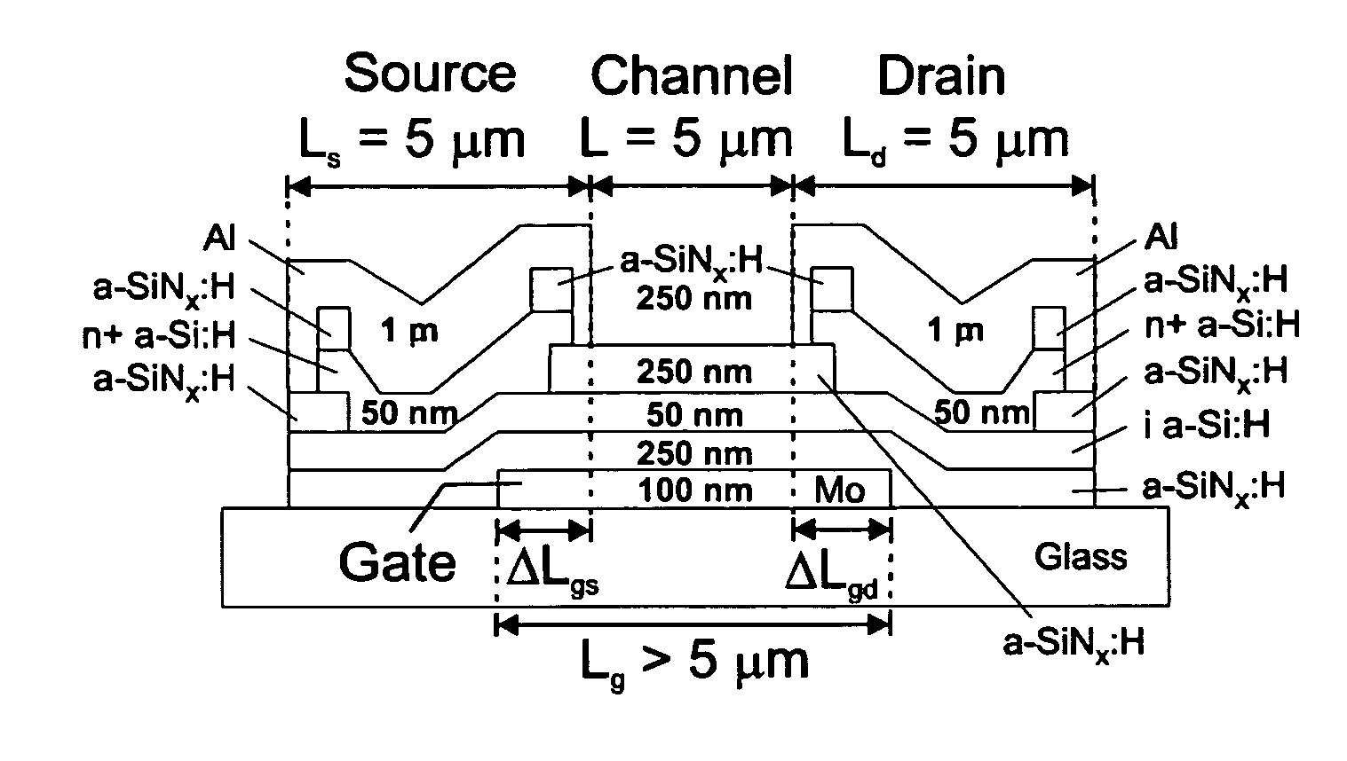
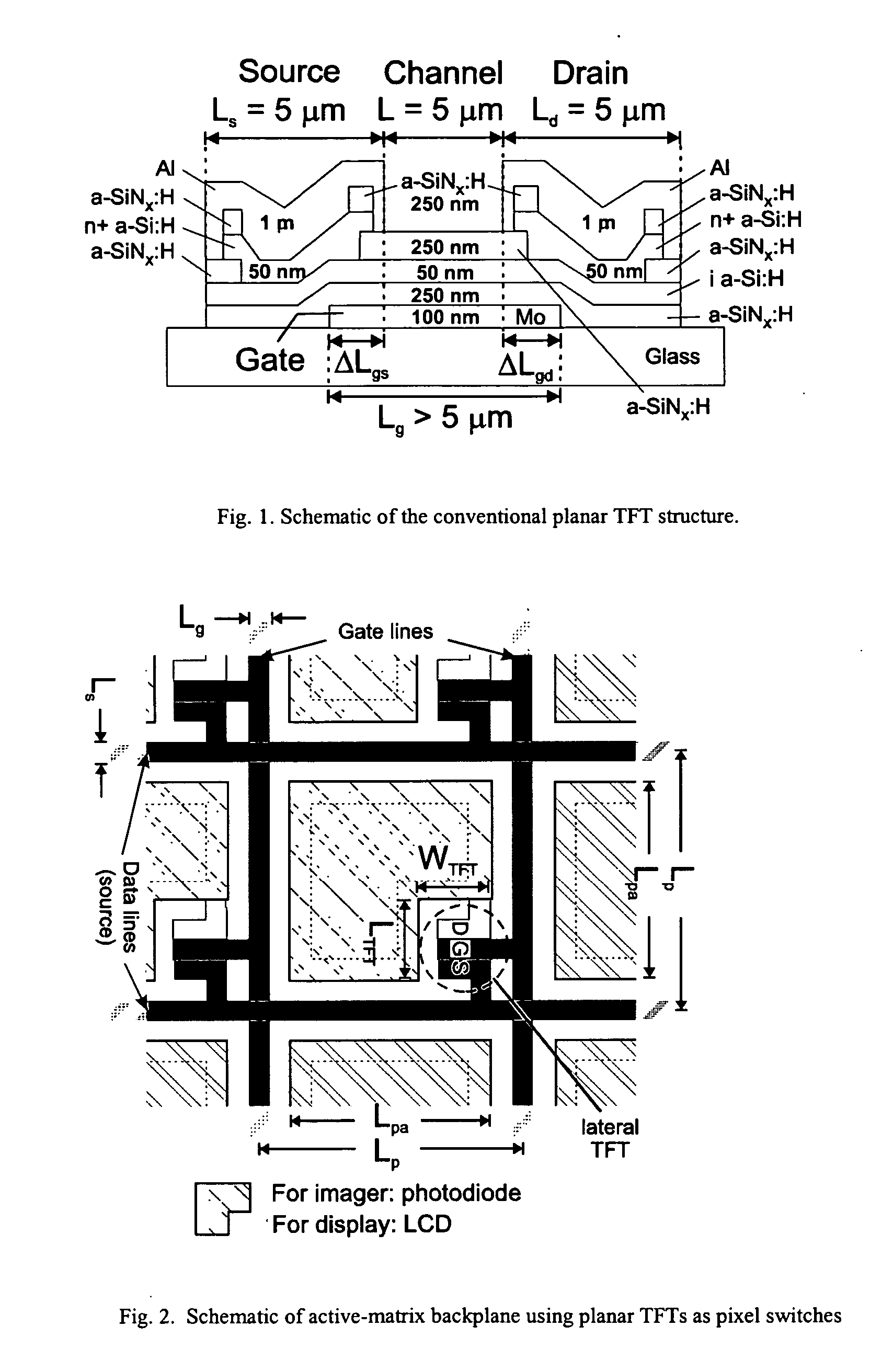
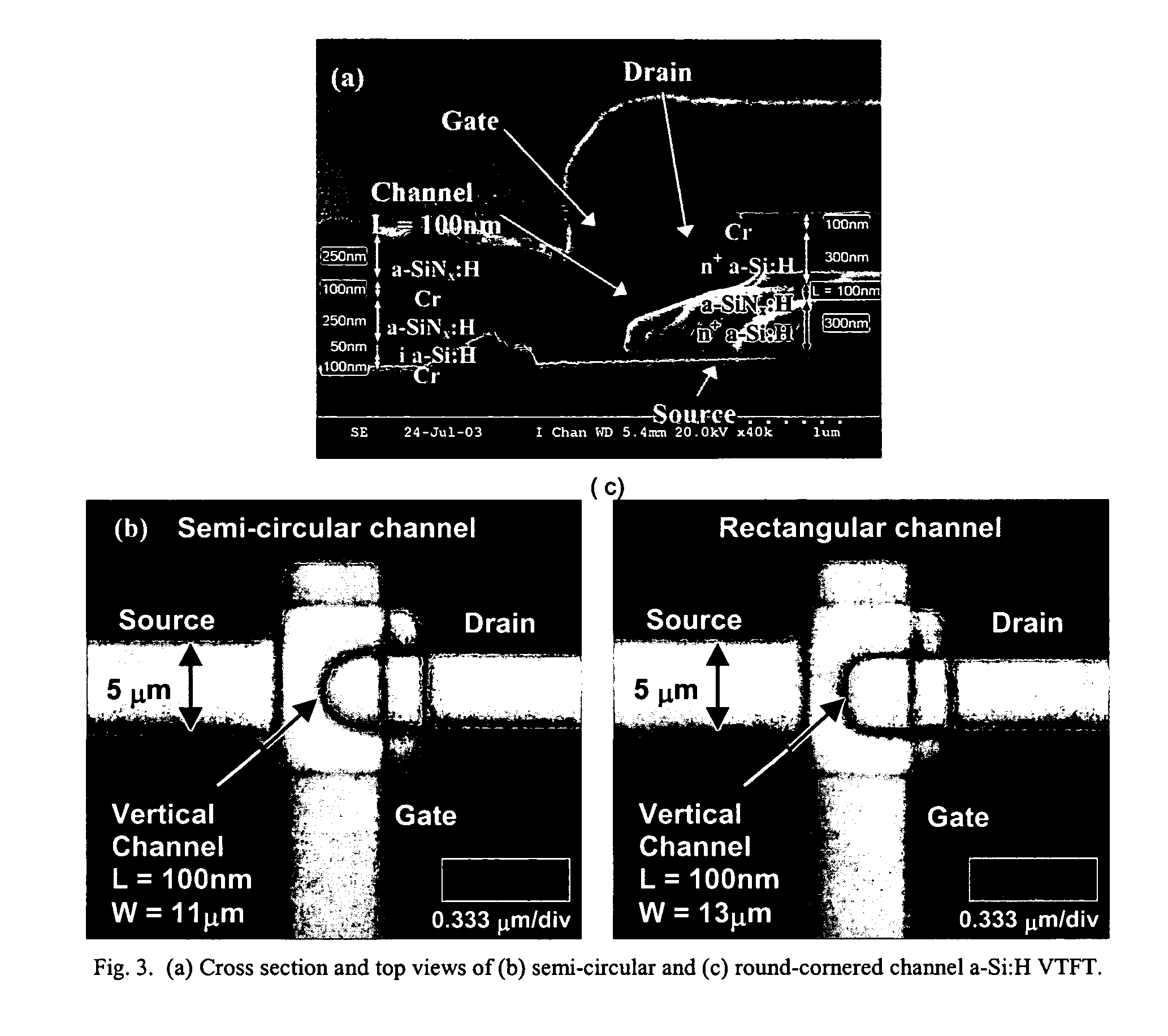
[0004] Disclosed here is the design of a new vertical thin film transistor (VTFT) using hydrogenated amorphous silicon (a-Si:H) technology. This design allows the channel length to be scaled down to nanometer-scale (100 nm and beyond) as well as the smallest possible TFT size on glass, plastic, or other common types of substrates, based on the standard photo-etching and thin film deposition processes [1],[2],[3],[4],[5]. The emphasis of using the standard processes for the new VTFTs has a strong implication that no additional process equipment and capital investments are required for technological advancements and gains in performance.
[0005] At the current state of art, lithographic technology is constrained to 5-μm or larger features [6] for large-area active-matrix imagers and displays, due to the stringent requirements of photo-etching precision and high yield on TFT and interconnect-line processes for virtually flawless images and low manufacturing cost. Consequently, advanced ...
PUM
 Abstract
Description
Claims
Application Information