Power composite integrated semiconductor device and manufacturing method thereof

a composite semiconductor and integrated technology, applied in semiconductor devices, semiconductor/solid-state device details, electrical apparatuses, etc., can solve problems such as reliability degradation, and achieve the effects of suppressing time-lapse degradation caused by copper, reducing resistance, and high bonding connection performan

Active Publication Date: 2005-11-24
DENSO CORP
View PDF5 Cites 53 Cited by
  • Summary
  • Abstract
  • Description
  • Claims
  • Application Information

AI Technical Summary

Benefits of technology

[0080] The above structure can implement the reduction in ON resistance at thick-film copper electrode portion of the power device portion, and the pad electrode is disposed on the active region of the control circuit portion (and power device portion), so that the power composite integrated semiconduct...

Problems solved by technology

The copper electrode needs to secure the bonding connection performance, and has a problem that diffus...

Method used


Image

  • Power composite integrated semiconductor device and manufacturing method thereof
  • Power composite integrated semiconductor device and manufacturing method thereof
  • Power composite integrated semiconductor device and manufacturing method thereof

Examples


first embodiment

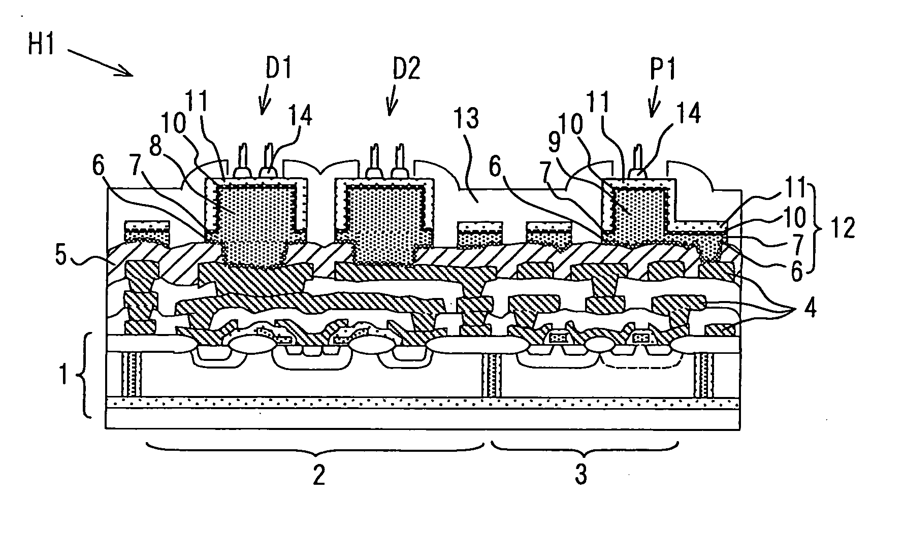
[0127]FIG. 1 is a diagram schematically showing a power composite integrated semiconductor device H1 according to a first embodiment of the present invention.

[0128] The power composite integrated semiconductor device H1 shown in FIG. 1 is a power composite integrated semiconductor device in which a power device portion 2 having a power device formed therein and a control circuit portion 3 having a control circuit formed therein are disposed in a composite style on a surface layer portion of one silicon substrate 1. The power device portion 2 and the control circuit portion 3 are connected by first wires 4 formed of aluminum or aluminum alloy disposed on the silicon substrate 1 so as to carry out desired control.

[0129] Furthermore, silicon nitride film 5 is formed as insulating film for covering and protecting the first wires 4, on the silicon substrate 1. The silicon nitride film 5 is greatly opened at the power element portion 2 so that the input / output thereof can collect curren...

second embodiment

[0149]FIG. 5 is a schematic diagram showing the cross-sectional structure of a power composite integrated semiconductor device H2 according to a second embodiment.

[0150] As in the case of the power composite integrated semiconductor device H1 shown in FIG. 1, the power composite integrated semiconductor device H2 shown in FIG. 5 is a power composite integrated semiconductor device in which a power device portion 141 having a power device formed therein and a control circuit portion 142 having a control circuit formed therein are arranged in a composite style on the surface layer portion of one silicon substrate 140. The device portion 141 and the control circuit portion 142 are wire-connected by first wires 143 formed of aluminum or aluminum alloy disposed on the silicon substrate 140 so as to perform desired control.

[0151] Silicon nitride film 144 is formed as insulating film for coating and protecting the first wires 143 on the silicon substrate 140. The silicon nitride film 144...

third embodiment

[0171] Before describing a third embodiment, the technique of forming the thick-film copper electrode by electroplating which is described in the first embodiment and the second embodiment will be described in more detail.

[0172] Electroplating using a resist or the like as a mask is generally used as a method of forming a thick-film electrode of copper having small specific resistance. In the mask plating, a planar copper electrode having high processing precision can be achieved by using a resist having high dimension precision as a mask.

[0173]FIG. 8 shows a current-concentrated state in the copper electroplating step. FIG. 9 shows the dependence of the film thickness of copper on the size of the opening.

[0174] As shown in FIG. 8, the current density in the electroplating step is varied in accordance with the area of the opening of the mask, and the current density is higher as the opening area is smaller. Due to the dependence of the current density on the opening area, there o...


PUM


Abstract

A high-reliability power composite integrated semiconductor device uses thick copper electrodes as current collecting electrodes of a power device portion to resist wire resistance needed for reducing ON-resistance. Furthermore, wire bonding connection of the copper electrodes is secured, and also the time-lapse degradation under high temperature which causes diffusion of copper and corrosion of copper is suppressed. Still furthermore, direct bonding connection can be established to current collecting electrodes in the power device portion, and also established to a bonding pad formed on the control circuit portion in the control circuit portion. A pad area at the device peripheral portion which has been hitherto needed is reduced, so that the area of the device is saved, and the manufacturing cost is reduced.

Description

CROSS REFERENCE TO RELATED APPLICATIONS [0001] This application is based upon, claims the benefit of priority of, and incorporates by reference the contents of Japanese Patent Application Nos. 2004-150745 filed on May 20, 2004 and 2004-328123 filed on Nov. 11, 2004. FIELD OF THE INVENTION [0002] The present invention relates to an integrated semiconductor device in which a power device and a control circuit are arranged in a composite style (hereinafter referred to as power composite integrated semiconductor device) and a method of manufacturing method thereof, and particularly to a power composite integrated semiconductor device that has a power device portion having a low ON-resistance, can be miniaturized and has high temperature reliability. BACKGROUND OF THE INVENTION [0003] (First Prior Art) [0004]FIG. 12 schematically shows a cross-sectional structure of a general conventional power composite integrated semiconductor device J1. In the power composite integrated semiconductor ...

Claims


Application Information

Patent Timeline
IPC IPC(8): H01L23/485H01L23/49H01L29/76
CPCH01L24/03H01L2924/0002H01L24/06H01L24/45H01L24/48H01L24/49H01L2224/04042H01L2224/05073H01L2224/05147H01L2224/05166H01L2224/05187H01L2224/05567H01L2224/05624H01L2224/05644H01L2224/45144H01L2224/48091H01L2224/48463H01L2224/48644H01L2224/48744H01L2224/48844H01L2224/49111H01L2224/49171H01L2224/49175H01L2224/49431H01L2924/01004H01L2924/01005H01L2924/01006H01L2924/01007H01L2924/01013H01L2924/01014H01L2924/01022H01L2924/01028H01L2924/01029H01L2924/01073H01L2924/01074H01L2924/01075H01L2924/01078H01L2924/01079H01L2924/014H01L2924/04941H01L2924/04953H01L2924/05042H01L2924/10253H01L2924/14H01L24/05H01L2224/0603H01L2224/05554H01L2924/01033H01L2224/45124H01L2224/45147H01L2224/48624H01L2224/02166H01L2224/05553H01L2924/00014H01L2924/00H01L2224/05552H01L2224/48824H01L2224/48724H01L2224/85375H01L2224/023H01L2924/00015H01L2924/0001
Inventor ITOU, HIROYASU
Owner DENSO CORP
Why Eureka
Try Eureka