MOSFET structure with high mechanical stress in the channel

Active Publication Date: 2005-11-24
AURIGA INNOVATIONS INC
View PDF5 Cites 29 Cited by
  • Summary
  • Abstract
  • Description
  • Claims
  • Application Information

AI Technical Summary

Benefits of technology

[0004] The application of stress changes the lattice dimensions of the silicon (Si)-containing substrate. By changing the lattice dimensions, the electronic band structure of the material is changed as well. This results in changes in carrier transport properties, which can be dramatic in certain cases. The application of stress can be used to enhance the performance of devices fabricated on the Si-containing substrates.
[0005] Compressive longitudinal stress along the channel increases drive current in p-type field effect transistors (pFETs) and decreases drive current in n-type field effect transistors (nFETs). Tensile longitudinal stress along the channel increases drive current in nFETs and decreases drive current in pFETs.
[0006] Nitride liners positioned atop field effect transistors (FETs) have been proposed as a means to provide stress

Problems solved by technology

However, there are growing signs today that metal oxide semiconductor transistors are beginning to reach their traditional scaling limits.
Since it has become increasingly difficult to improve MOSFETs and therefore CMOS performance through continued scaling, methods for improving performance without scaling have become critical.
This results in changes in

Method used


Image

  • MOSFET structure with high mechanical stress in the channel
  • MOSFET structure with high mechanical stress in the channel
  • MOSFET structure with high mechanical stress in the channel

Examples


Embodiment Construction

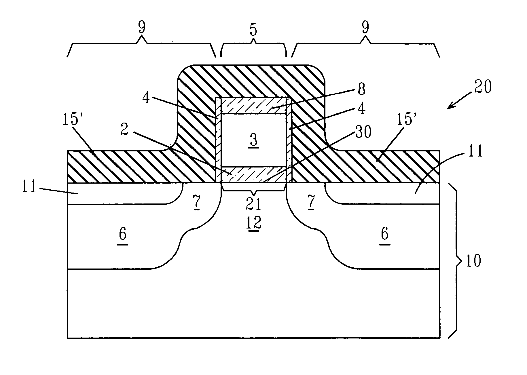
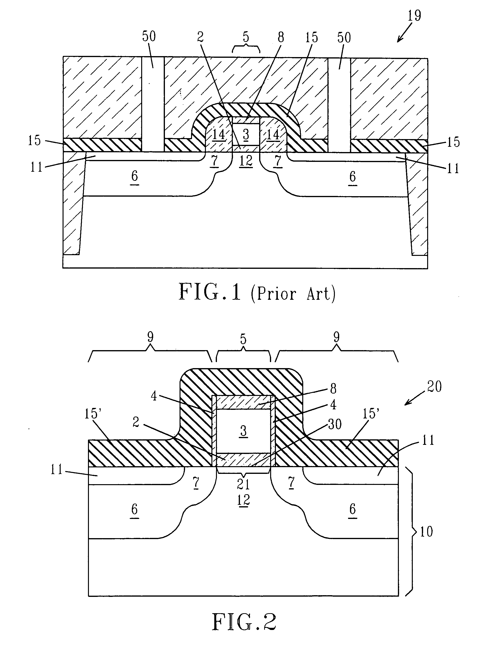
[0035] The present invention provides a field effect transistor (FET), and a method of forming thereof, comprising a gate structure on a semiconducting substrate, in which a longitudinal stress is applied to a portion of the semiconducting substrate underlying the gate region to increase the FET's performance. The present invention advantageously provides a longitudinal stress to the portion of the substrate underlying the gate region by forming a stress inducing liner positioned in close proximity to the gate region and atop a surface of the substrate adjacent to and planar with the portion of the substrate on which the gate region is formed. The present invention is now discussed in more detail referring to the drawings that accompany the present application. In the accompanying drawings, like and / or corresponding elements are referred to by like reference numbers. In the drawings, a single gate region is shown and described. Despite this illustration, the present invention is not...


PUM


Abstract

The present invention provides a semiconducting device including at least one gate region including a gate conductor located on a surface of a substrate, the substrate having an exposed surface adjacent the gate region; a silicide contact located adjacent the exposed surface; and a stress inducing liner located on the silicide contact, the exposed surface of the substrate adjacent to the gate region and the at least one gate region, wherein the stress inducing liner provides a stress to a device channel portion of the substrate underlying the gate region. The stress produced on the device channel is a longitudinal stress on the order of about 200 MPa to about 2000 MPa. The present invention also provides a method for forming the above-described semiconducting device.

Description

FIELD OF THE INVENTION [0001] The present invention relates to semiconductor devices having enhanced electron and hole mobilities, and more particularly, to semiconductor devices that include a silicon (Si)-containing layer having enhanced electron and hole mobilities. The present invention also provides methods for forming such semiconductor devices. BACKGROUND OF THE INVENTION [0002] For more than three decades, the continued miniaturization of silicon metal oxide semiconductor field effect transistors (MOSFETs) has driven the worldwide semiconductor industry. Various showstoppers to continued scaling have been predicated for decades, but a history of innovation has sustained Moore's Law in spite of many challenges. However, there are growing signs today that metal oxide semiconductor transistors are beginning to reach their traditional scaling limits. A concise summary of near-term and long-term challenges to continued complementary metal oxide semiconductor (CMOS) scaling can be...

Claims


Application Information

Patent Timeline
IPC IPC(8): H01L21/336H01L21/8234H01L21/8238H01L29/78
CPCH01L21/823807H01L29/6653H01L29/7843H01L29/7833H01L29/6659
Inventor CHEN, XIANGDONGCHIDAMBARRAO, DURESETIGLUSCHENKOV, OLEGGREENE, BRIANRIM, KERNYANG, HAINING S.
Owner AURIGA INNOVATIONS INC
Why Eureka
Try Eureka