Ultraviolet ray generator, ultraviolet ray irradiation processing apparatus, and semiconductor manufacturing system
a technology of ultraviolet rays and processing equipment, applied in nuclear engineering, spectrometry/spectrophotometry/monochromators, optical radiation measurement, etc., can solve the problem of reducing the mechanical strength of the entire film, unable to achieve the relative dielectric constant of 2.5 or less by a single material, and unable to withstand a polishing process
- Summary
- Abstract
- Description
- Claims
- Application Information
AI Technical Summary
Benefits of technology
Problems solved by technology
Method used
Image
Examples
first embodiment
Explanation of the Ultraviolet Ray Generator that is the Present Invention
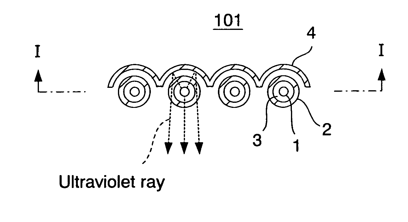
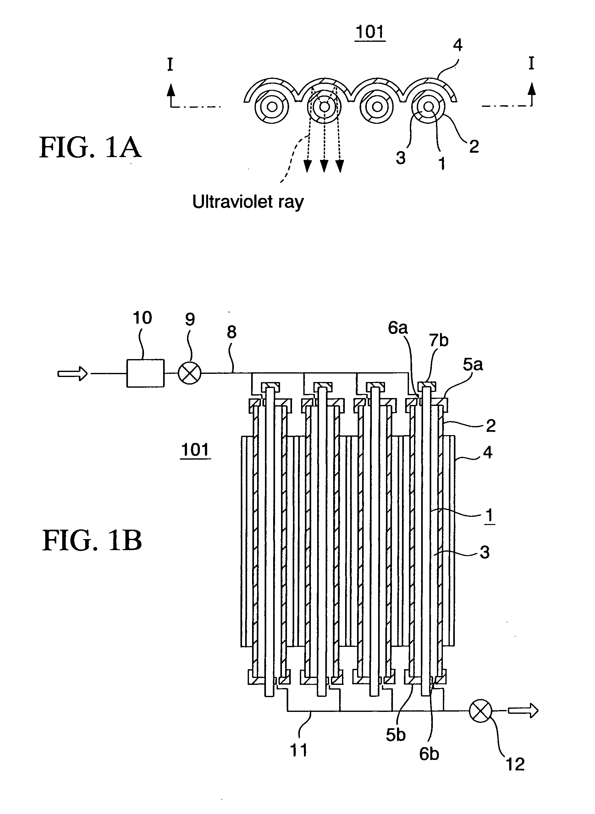
[0038]FIG. 1A is the side view showing the constitution of the ultraviolet ray generator according to the first embodiment of the present invention. FIG. 1B is the cross-sectional view taken along I-I line of FIG. 1A.
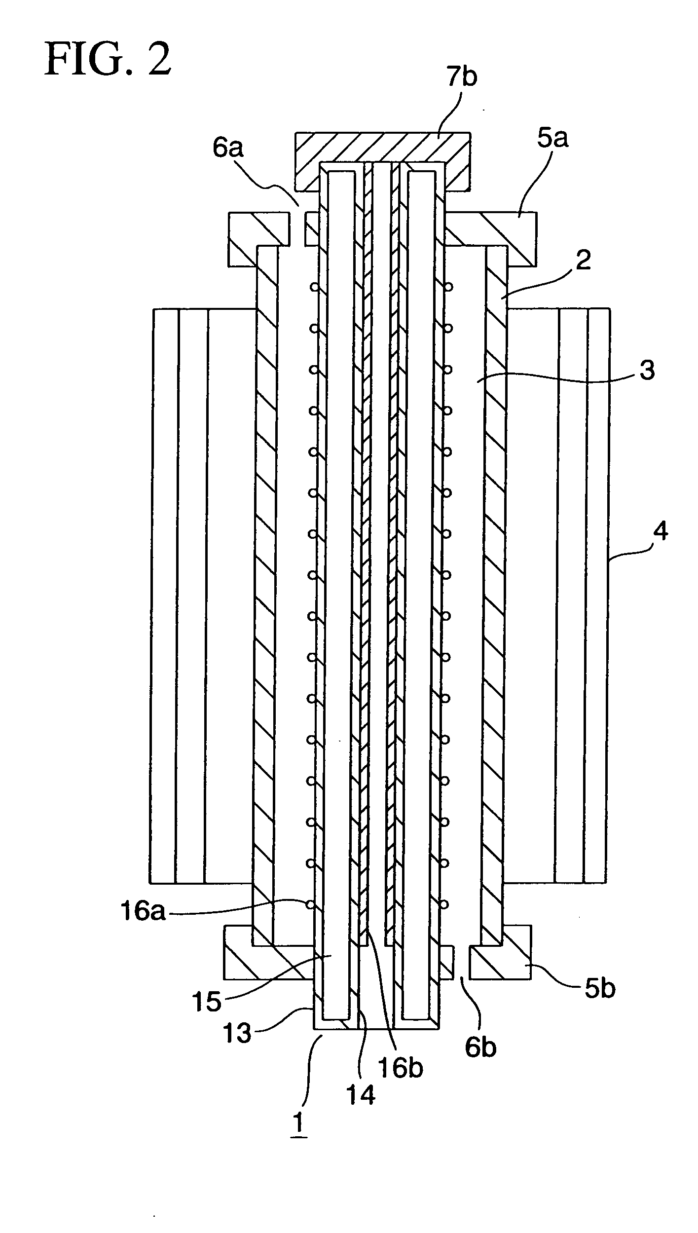
[0039] The ultraviolet ray generator 101, as shown in FIGS. 1A and 1B, is provided with main bodies of four columnar ultraviolet ray lamps 1, four tubular protective tubes 2 made of quartz glass (material that transmits ultraviolet ray), each of which individually houses each ultraviolet ray lamp 1 and separates the ultraviolet ray lamp 1 from outside, and an ultraviolet ray reflective plate 4 that allows ultraviolet ray radially generated from the ultraviolet ray generator to travel in a specific direction (downward in FIG. 1A) by reflection. Note that the specific direction does not mean that all ultraviolet rays travel in a specific direction at a same angle, but means that the rays are allowe...
second embodiment
Explanation of the Ultraviolet Ray Irradiation Processing Apparatus that is the Present Invention
[0052]FIG. 3 is the side view showing the constitution of an ultraviolet ray irradiation processing apparatus 102 according to the second embodiment of the present invention.
[0053] The ultraviolet ray irradiation processing apparatus 102, as shown in FIG. 3, has a load lock chamber 32 that can be decompressed, a transfer chamber 33 that can be decompressed, and an ultraviolet ray irradiation processing chamber 21 that can be decompressed, and the chambers (32, 33, 21) are connected in series in this order. Communication / non-communication between the chambers is performed by open / close of gate valves (34b, 34c). In other words, the apparatus is capable of continuously performing ultraviolet ray irradiation processing and anneal processing in the low-pressure atmosphere without exposing a substrate 42 to the atmosphere.
[0054] The load-lock chamber 32 corresponds to an entrance / exit of th...
third embodiment
Explanation of the Semiconductor Manufacturing System that is the Present Invention
[0072] In the semiconductor manufacturing system of the present invention, there is a possibility of the combination of the ultraviolet ray irradiation processing apparatus according to the second embodiment whose heating device has been omitted, and the heating apparatus, the combination of the film forming apparatus and the ultraviolet ray irradiation processing apparatus of the second embodiment (when the heating device is provided), or the combination of the film forming apparatus and the ultraviolet ray irradiation processing apparatus of the second embodiment (when the heating device is not provided), and the systems can be constituted such that the constituent apparatus of each combination are connected in series in order or connected in parallel via the transfer chamber. A chemical vapor deposition apparatus (CVD apparatus) or a coating apparatus can be used as the film forming apparatus.
[007...
PUM
| Property | Measurement | Unit |
|---|---|---|
| Shape | aaaaa | aaaaa |
| Transparency | aaaaa | aaaaa |
| Wavelength | aaaaa | aaaaa |
Abstract
Description
Claims
Application Information


