Light scattering euvl mask

a light scattering and radiation reflective mask technology, applied in the field of reflective masks, to achieve the effect of reducing mask reflectivity, reducing mask contrast, and increasing reflectivity

Inactive Publication Date: 2005-12-01
GLOBALFOUNDRIES INC
View PDF9 Cites 18 Cited by
  • Summary
  • Abstract
  • Description
  • Claims
  • Application Information

AI Technical Summary

Benefits of technology

[0014] The invention eliminates the need for a buffer or absorber layer within the mask stack and overcomes the problems inherent with conventional EUVL masks previously described. Because the multilayer is deposited as the final step in the mask fabrication, the multilayer will not be subjected to the plasma etches, wet etches, and multiple cleans that degrade the multilayer in the standard EUVL mask process and consequently reduce the mask reflectivity. In this invention, the higher reflectivity increases the mask contrast between reflective and scattering regions, decreases the required exposure time, and reduces the amount of radiation that is absorbed by the mask.
[0015] The inventive mask comprises a substrate (which may include a bonded crystalline Si layer) and the multilayer without an absorber or buffer layer. The absence of a raised absorber stack eliminates the shadow effect during wafer printing. This results in an abrupt transition from dark to reflective mask regions and the effect is an improvement in the edge contrast on the lithographic wafer.

Problems solved by technology

However, in regions where the EUV radiation is not intended to reach the surface of the wafer, the topography is configured such that it scatters the radiation out of the imaging optics of the stepper and hence would not print.

Method used


Image

  • Light scattering euvl mask
  • Light scattering euvl mask
  • Light scattering euvl mask

Examples


Embodiment Construction

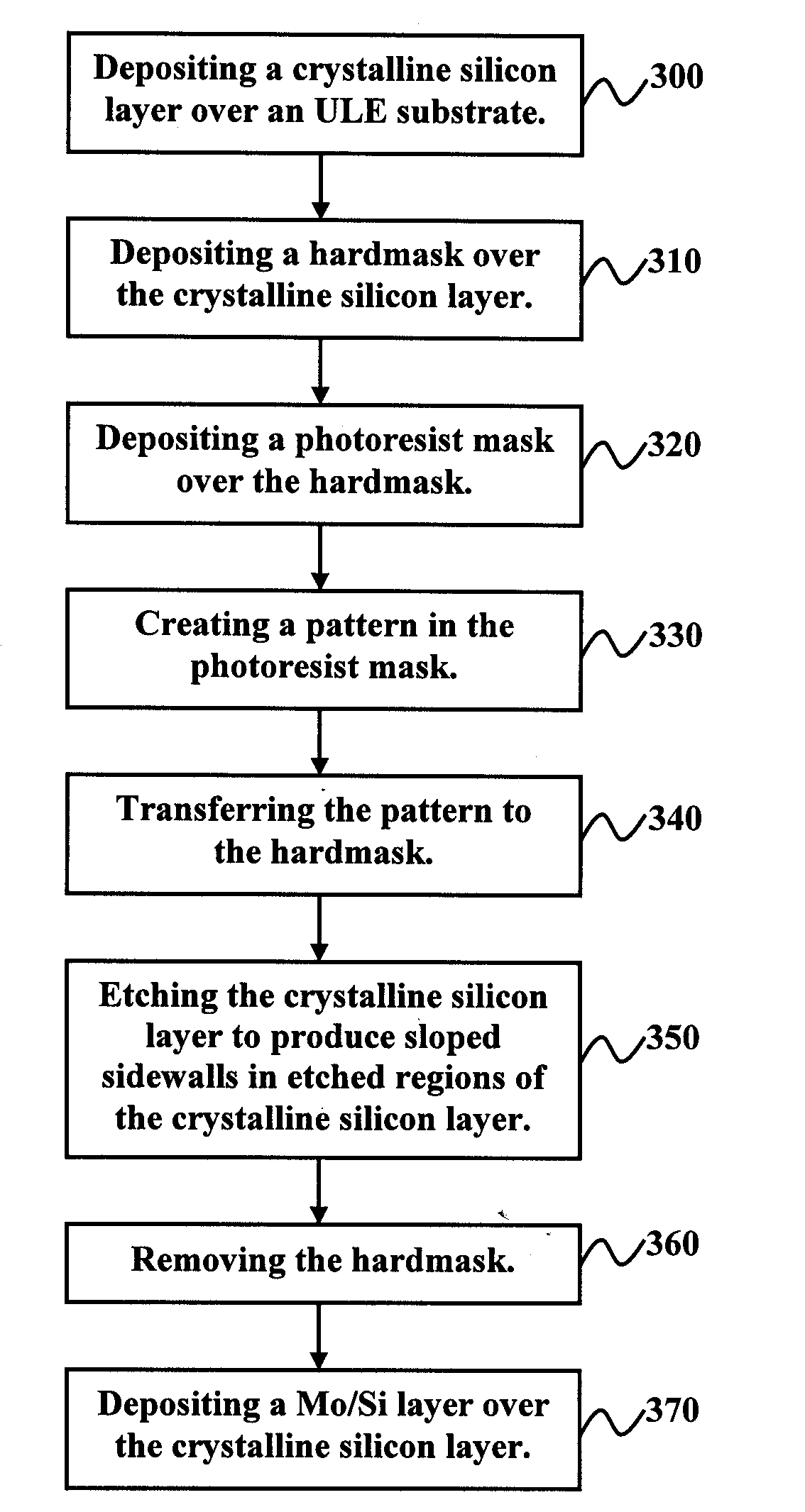
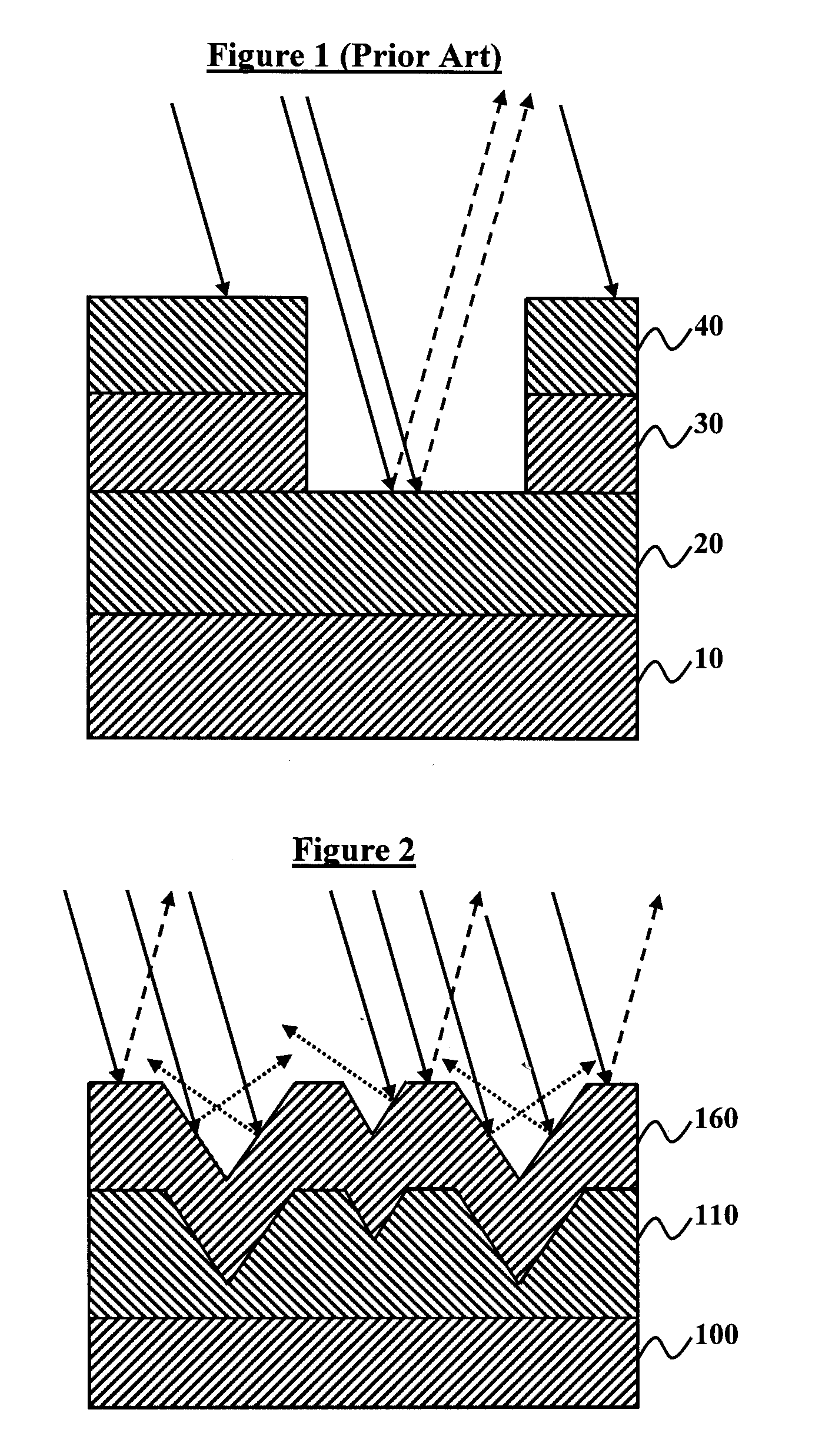
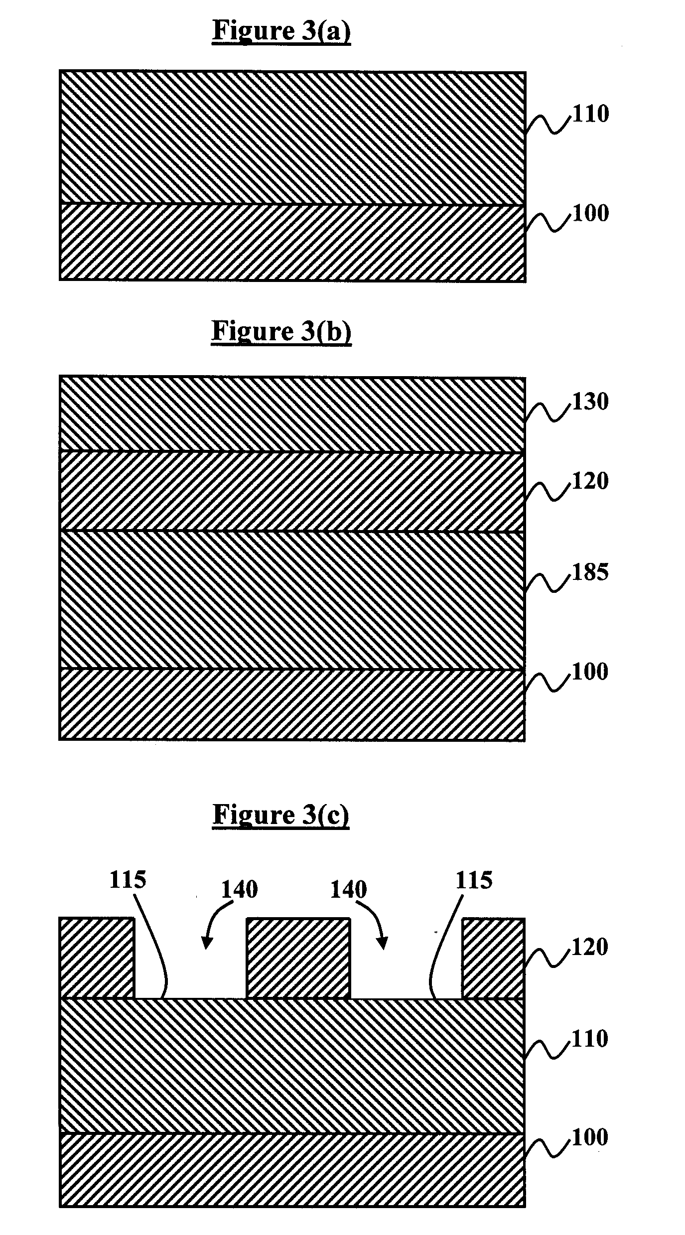
[0023] The invention and the various features and advantageous details thereof are explained more fully with reference to the non-limiting embodiments that are illustrated in the accompanying drawings and detailed in the following description. It should be noted that the features illustrated in the drawings are not necessarily drawn to scale. Descriptions of well-known components and processing techniques are omitted so as to not unnecessarily obscure the invention. The examples used herein are intended merely to facilitate an understanding of ways in which the invention may be practiced and to further enable those of skill in the art to practice the invention. Accordingly, the examples should not be construed as limiting the scope of the invention.

[0024] As previously mentioned, there is a need for a novel EUVL mask and method of manufacturing an EUVL mask, which overcomes the problems associated with the standard masks and associated manufacturing techniques. Referring now to the...


PUM

PropertyMeasurementUnit
angleaaaaaaaaaa
wavelengthaaaaaaaaaa
angleaaaaaaaaaa

Abstract

A light scattering EUVL mask and a method of forming the same comprises depositing a crystalline silicon layer over an ultra low expansion substrate, depositing a hardmask over the crystalline silicon layer, patterning the hardmask; etching the crystalline silicon layer, removing the hardmask, and depositing a Mo/Si layer over the crystalline silicon layer, wherein etched regions of the crystalline silicon layer comprise uneven surfaces in the etched regions. The method further comprises depositing a photoresist mask over the hardmask, creating a pattern in the photoresist mask, and transferring the pattern to the hardmask. The Mo/Si layer comprises uneven surfaces conformal with the sloped surfaces of the crystalline silicon layer, wherein the sloped surfaces of the Mo/Si layer may be configured as roughened, jagged, sloped, or curved surfaces, wherein the uneven surfaces deflect incoming extreme ultraviolet radiation waves to avoid collection by exposure optics and prevent printing onto a semiconductor wafer.

Description

BACKGROUND OF INVENTION [0001] 1. Field of the Invention [0002] The invention generally relates to reflective masks, and more particularly to a light scattering and radiation reflective EUVL mask. [0003] 2. Description of the Related Art [0004] The optical lithographic technique that is used to image wafers throughout the semiconductor industry relies on transparent masks to transfer an image from the mask to the wafer. As wafer images shrink, new ways of imaging the wafer resist are needed. One likely candidate for the Next Generation Lithography uses Extreme Ultraviolet (EUV) light to image. At the 13.4 nm EUV wavelength, materials are too absorptive to build a transmissive mask, so reflective ones are used instead. Conventional Extreme Ultraviolet Lithography (EUVL) masks, such as the mask illustrated in FIG. 1, are built by depositing a reflective film onto an ultra low expansion (ULE) substrate 10. Material properties of ULE substrates are well known in the art. This film can b...

Claims


Application Information

Patent Timeline
Patent Type & Authority Applications(United States)
IPC IPC(8): B32B9/00B32B15/00B32B17/06G03C5/00G03F1/00G03F1/14G21K1/06G21K5/00
CPCB82Y10/00B82Y40/00G21K2201/067G21K1/062G03F1/24G03F1/38
Inventor GALLAGHER, EMILY E.KINDT, LOUIS M.THIEL, CAREY W.
Owner GLOBALFOUNDRIES INC
Why Eureka
Try Eureka