Method for producing substantially planar films

a technology of substantially planar films and substrates, applied in the direction of superconductor devices, vacuum evaporation coating, semiconductor/solid-state device details, etc., can solve the problems of large-scale ic fabrication processes, inconvenient use of impedance matching networks, and insufficient high-quality sputter-deposited sio/sub>2/sub> alone,

a technology of substantially planar films and substrates, applied in the direction of superconductor devices, vacuum evaporation coating, semiconductor/solid-state device details, etc., can solve the problems of large-scale ic fabrication processes, inconvenient use of impedance matching networks, and insufficient high-quality sputter-deposited sio/sub>2/sub> alone,

US20050267000A1Inactive Publication Date: 2005-12-01KERBER GEORGE L

Image

  • Method for producing substantially planar films
  • Method for producing substantially planar films
  • Method for producing substantially planar films

Examples


example 1

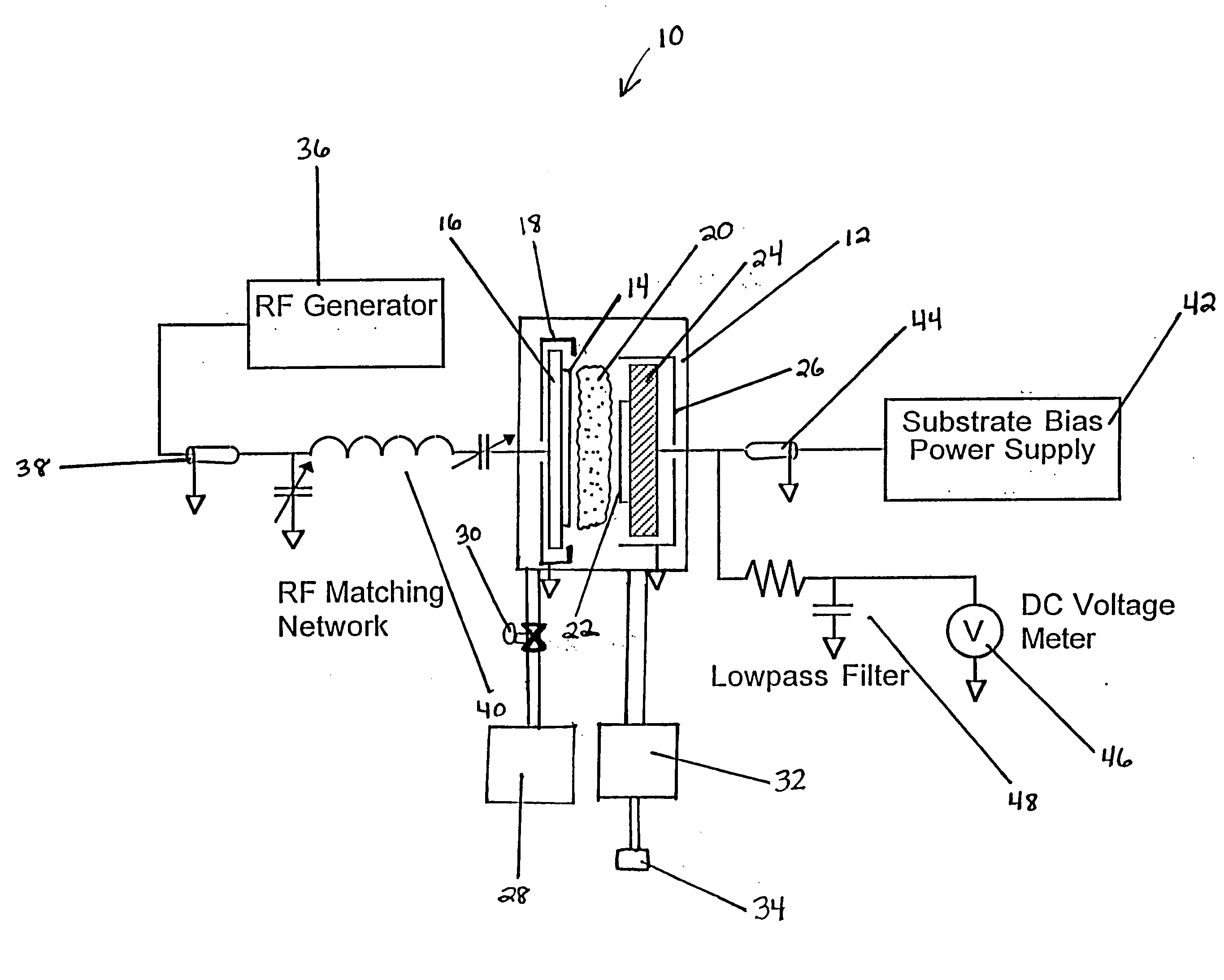
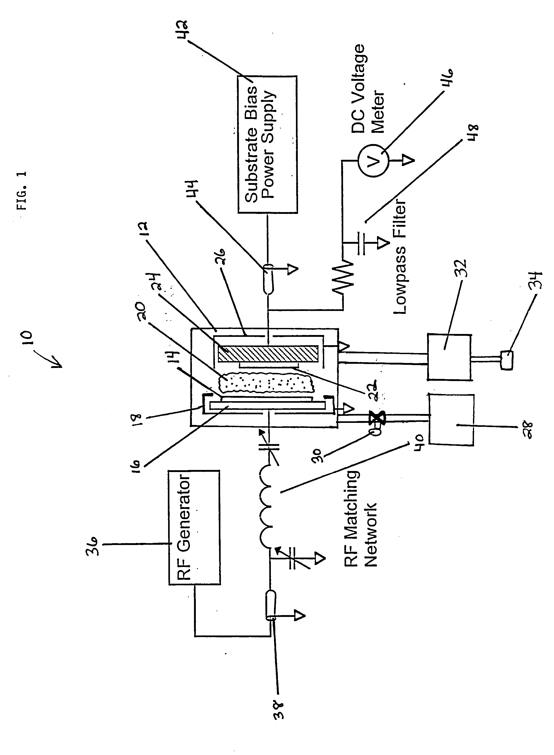
[0066] In this example, the apparatus shown in FIG. 1 was used for sputter deposition of a substrate coated with a niobium nitride (NbN) metal layer. First, a niobium nitride (NbN) metal film was sputter deposited in a conventional sputter deposition machine on a silicon wafer having a diameter of about 75 mm and having a thickness of about 0.5 mm. The NbN film used was a polycrystalline superconductive film having a Tc (transition temperature) of 15.4 K (Kelvin).

[0067] The coated silicon substrate had an NbN layer thickness of 500 nm. The roughness of the NbN layer was about 4.2 nm (rms) as measured by atomic force microscope. The peak-to-valley roughness of the NbN film was approximately 15 nm to 20 nm, as measured by atomic force microscope.

[0068] After, the substrate was coated with the NbN film layer, the coated substrate was mounted to a substrate holder within the reaction chamber of the apparatus 10 shown in FIG. 1 The substrate was positioned about 17.8 cm from a silicon ...


PUM

PropertyMeasurementUnit
Nanoscale particle sizeaaaaaaaaaa
Frequencyaaaaaaaaaa
Frequencyaaaaaaaaaa

Abstract

This present invention is directed to a method for producing very smooth, substantially planar films for use in the manufacture of high performance superconductive integrated circuits (ICs) and in the fabrication of tunnel junctions. The method of the present invention applies a low frequency AC bias voltage to a substrate and uses a sputtered target material, such as silicon dioxide, to effectively produce very smooth and substantially planar films, and in particular, oxide films and metal films. The method produces films, such as oxide films, on a bare or uncoated substrate, the films having a surface roughness of less than about 0.1 nanometer. The method also produces films on a conductive or coated substrate, the films having a surface roughness of less than about 1.0 nanometer.

Description

BACKGROUND OF THE INVENTION [0001] 1. Field of the Invention [0002] This invention relates generally to a method for producing substantially planar films, and more particularly, to a method for producing very smooth, substantially planar films, such as oxide and metal films, for use in the manufacture of high performance superconductive integrated circuits (ICs) and in the fabrication of tunnel junctions. [0003] 2. Discussion of the Related Art [0004] Thin films, such as oxide films and metal films, are used in the manufacture of superconductive integrated circuits (ICs), in the fabrication of tunnel junctions, and in related applications. It is desirable to form such films having a smooth, and planar or substantially planar surface, resulting in improved interconnect wiring reliability in integrated circuits, increased performance and yield and decreased subgap leakage in tunnel junctions, reduced defect density of the films, and improved step coverage. [0005] Thin films may be for...

Claims


Application Information

Patent Timeline
01 Dec 2005
Publication
US20050267000A1
IPC
C23C14/10; C23C14/02; C23C14/34; C23C14/40; H01G2/00; H01L21/203; H01L21/316; H01L27/18; H01L39/24
CPC
C23C14/10; H01L27/18; H01L21/316; H01L21/2855; H01L21/02266; H01L21/02164; H01L21/02192; H10N69/00
Inventors
KERBER, GEORGE L.