
Film forming apparatus and film forming method

a film forming and film technology, applied in the direction of coatings, chemical vapor deposition coatings, metallic material coating processes, etc., can solve the problems of large installation space, inability to form flat films, and process not being effectively performed in a long time, so as to reduce the installation space of the facility

Inactive Publication Date: 2005-12-08
TOKYO ELECTRON LTD
View PDF12 Cites 12 Cited by
  • Summary
  • Abstract
  • Description
  • Claims
  • Application Information

AI Technical Summary

Benefits of technology

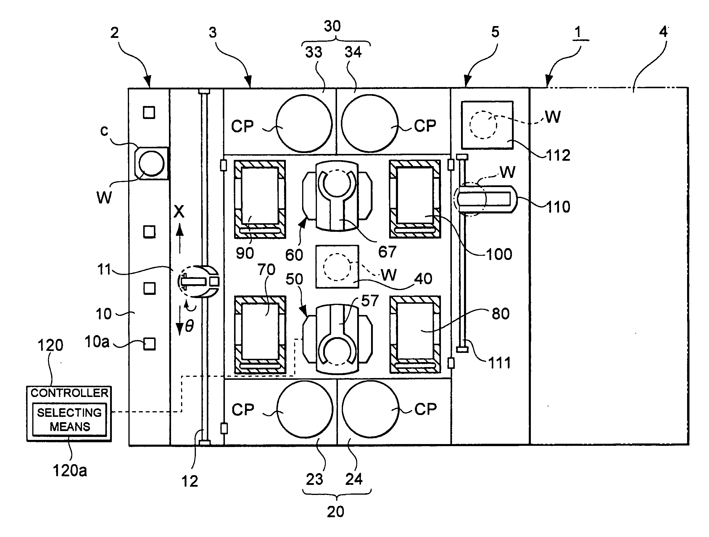
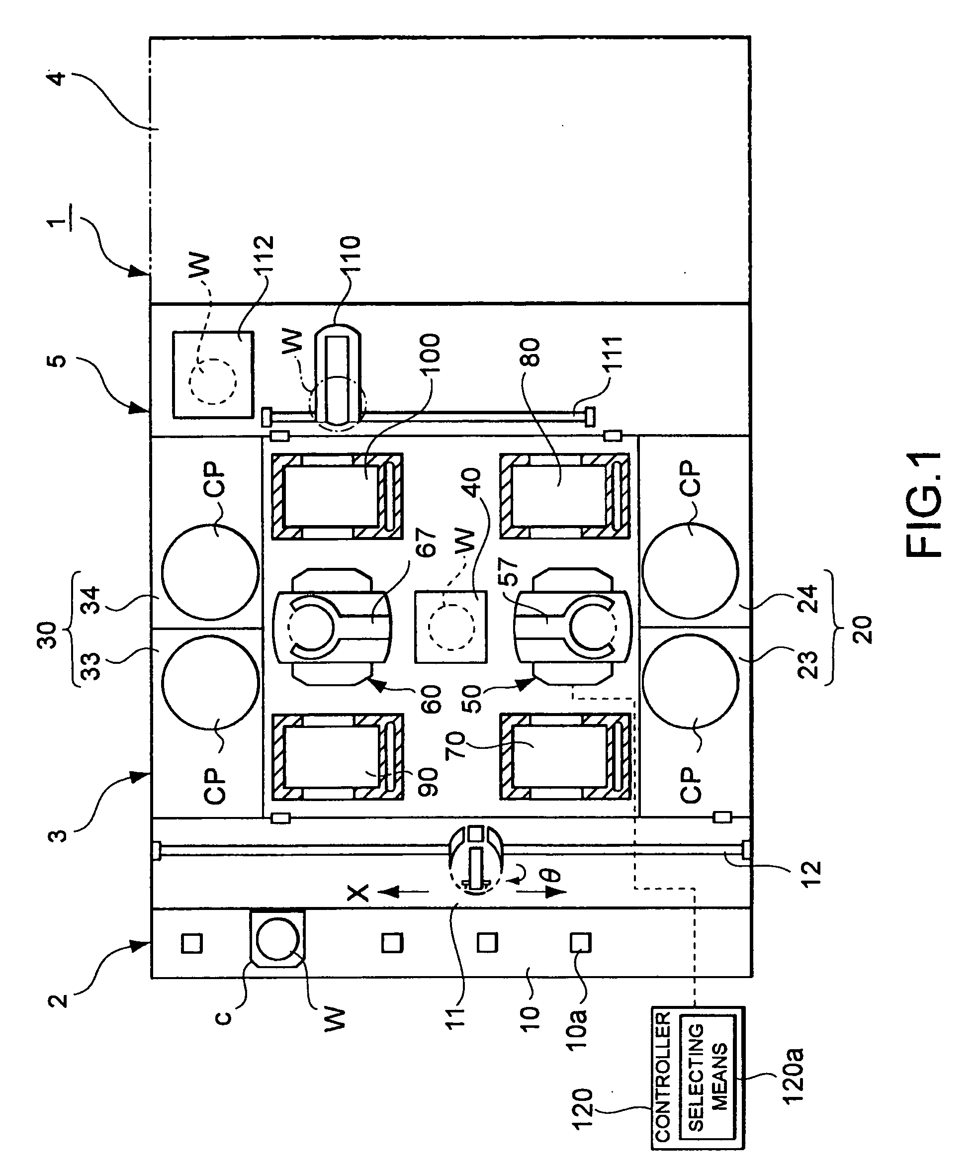
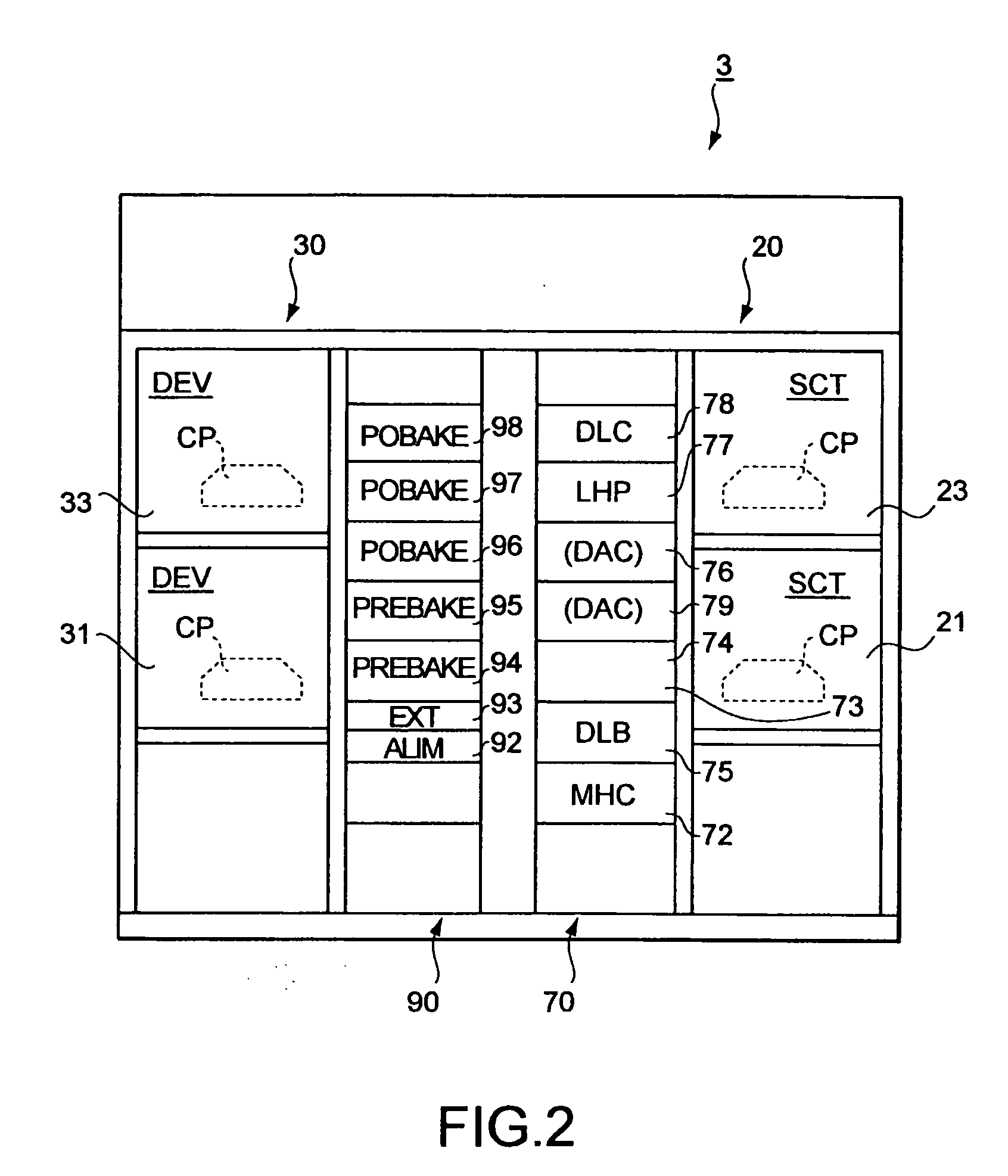
[0008] The present invention is made from the above-described point of view. An object of the present invention is to provide a film forming apparatus and a film forming method that allow the installation space of the facility to be reduced and a laminate film made of a porous insulation film and a non-porous insulation film to be effectively formed.
[0011] According to the present invention, with providing the selecting means that selects processing apparatuses to which the wafer W is transferred corresponding to a type of film formed on the substrate, film forming processes for a porous insulation film and a non-porous insulation film can be performed in the same system. Thus, unlike the conventional system, it is not necessary to transfer the substrate between different systems. As a result, film forming processes can be effectively performed. Thus, the installation space of the apparatus can be reduced. As a result, the time taken for processing can be shortened.
[0013] According to the present invention, the first coating apparatus coats a porous insulation material with the spin coat process and the second coating apparatus coats a non-porous insulation material with the spin coat process. Thus, even if the front surface of the porous insulation film is largely rugged (namely, the surface roughness thereof is large), the non-porous insulation film as an upper layer can be flatly formed. In addition, since all the processes including the heating process of the first heating apparatus and the second heating apparatus are performed in the same apparatus that has a transferring mechanism, unlike the conventional art, it is not necessary to transfer a substrate between different systems. As a result, the film forming processes can be effectively performed. Thus, the installation space of the apparatus can be reduced. As a result, the time taken for processing can be shortened.
[0017] Another example of the present invention further comprising the step (e) of reforming a front surface of the first insulation film, the step (e) being performed between the steps (b) and (c). In this example, the reforming process is performed by radiating an ultraviolet ray to the first insulation film. With such reforming process, the water absorption of the front surface of the film is improved and the film becomes hydrophilic. As a result, the contact angle of the non-porous insulation film material to the porous insulation film becomes small, therefore, the non-porous material can be easily coated. In other words, when a non-porous insulation material is spread on a substrate by the spin coat process, the material can easily be spread and flattened. In addition, since the material can easily be spread, the amount required of the material can be reduced.
[0018] Another embodiment of the present invention comprises the step of coating a solvent on the first insulation film with the spin coat process, after the reforming process. Thus, water absorption of the front surface of the porous film can be improved further. When a non-porous insulation material is spread on a substrate by the spin coat process, the material can easily be spread and flattened. In addition, since the material can easily be spread, the amount required of the material can be reduced.

Problems solved by technology

Thus, the facility becomes large.
In addition, a wafer has to be transferred between the systems and, as a result, the process is not effectively performed taking a long time to complete.
As a result, a flat film cannot be formed.

Method used


Image

  • Film forming apparatus and film forming method
  • Film forming apparatus and film forming method
  • Film forming apparatus and film forming method

Examples


Embodiment Construction

[0034] Next, with reference to the accompanying drawings, an embodiment of the present invention will be described.

[0035] In the embodiment, a fabrication method for a semiconductor device having a laminated film composed of three layers of insulation films in FIG. 5D will be described.

[0036] As shown in FIG. 5D, a lower layer wiring 201 is formed on a semiconductor wafer W (hereinafter abbreviated as wafer W). On the lower layer wiring 201, an inter-layer insulation film composed of layers of laminated films is formed. The inter-layer insulation film is composed of a porous insulation film 202, a non-porous insulation film 203, and a porous insulation film 204. A porous insulation film is a film made with processing a foaming material. In the inter-layer insulation film, for example through-holes (not shown) are formed. Via the through-holes, a wiring (not shown) that is made of a conductive material and formed on the inter-layer insulation film and the lower layer wiring 201 are...


PUM


Abstract

An apparatus for forming a film on a wafer comprising, a first coating apparatus coating a foaming insulation film material on the wafer, a second coating apparatus coating a non-porous insulation film material on the wafer, a low oxygen heating temperature regulating process apparatus performing a heating process on the wafer on which the foaming insulation film material is coated, a low oxygen high temperature heating process apparatus performing the heating process on the water on which the non-foaming insulation film material is coated, a transfer mechanism transferring the wafer to these apparatuses, and a selecting means selecting a path to which the wafer is transferred corresponding to the film formed on the wafer.

Description

BACKGROUND OF THE INVENTION [0001] 1. Field of the Invention [0002] The present invention relates to a film forming apparatus that forms a porous insulation film and a non-porous insulation film on a substrate such as a semiconductor wafer. [0003] 2. Description of the Related Art [0004] An insulation film is formed on a substrate in such a manner that an insulation film material is coated on the substrate, dried, and heated. A system that integrally performs a series of processing steps such as a coating process, a drying process, and a heating process for an insulation film material is known. [0005] Recently, the improvement of the insulating characteristic of an insulation film has been required. In order to meet the requirement, a porous insulation film has been used. For such a coating material, a material such that contains porogen in an insulation film material like methyl silsesquioxane (hereinafter abbreviated as MSQ) is used. In addition, after the coating process for such...

Claims


Application Information

Patent Timeline
IPC IPC(8): H01L21/00
CPCH01L21/6715H01L21/67225H01L21/67207H01L21/67178
Inventor ISHIDA, HIROSHI
Owner TOKYO ELECTRON LTD
Learn More