Supercharge Your Innovation With Domain-Expert AI Agents!

Data processing system and data processing method

a data processing system and data processing technology, applied in the field of data processing system and data processing method, can solve the problems of reducing the use efficiency of each storage area in particular, affecting the accuracy of data rewriting, so as to improve the number of rewrite assurances, write or programming time, and increase the thickness of gate oxide film

Inactive Publication Date: 2005-12-22
RENESAS TECH CORP +1
View PDF14 Cites 42 Cited by
  • Summary
  • Abstract
  • Description
  • Claims
  • Application Information

AI Technical Summary

Benefits of technology

"The present invention provides a data processing system that optimizes the use of storage areas by error correcting information, such as ECC codes, to enhance the reliability of stored information. The system can select an ECC method that matches with a device characteristic to reduce overhead of each ECC code and increase the use efficiency of each storage area to a maximum. This system can also reduce the number of errors and improve the number of assurances for rewriting stored information."

Problems solved by technology

Therefore, the use efficiency of each storage area is greatly impaired.
When the amount of data to be frequently rewritten is low, a reduction in the use efficiency of each storage area in particular would bedome pronounced.
According to the discussion of the present inventors, it became evident that the versatility of the selection of the ECC method was hard to be easily implemented where the generation of the ECC codes or the error detection and correction were achieved by hardware.

Method used


Image

  • Data processing system and data processing method
  • Data processing system and data processing method
  • Data processing system and data processing method

Examples


embodiment 1

>

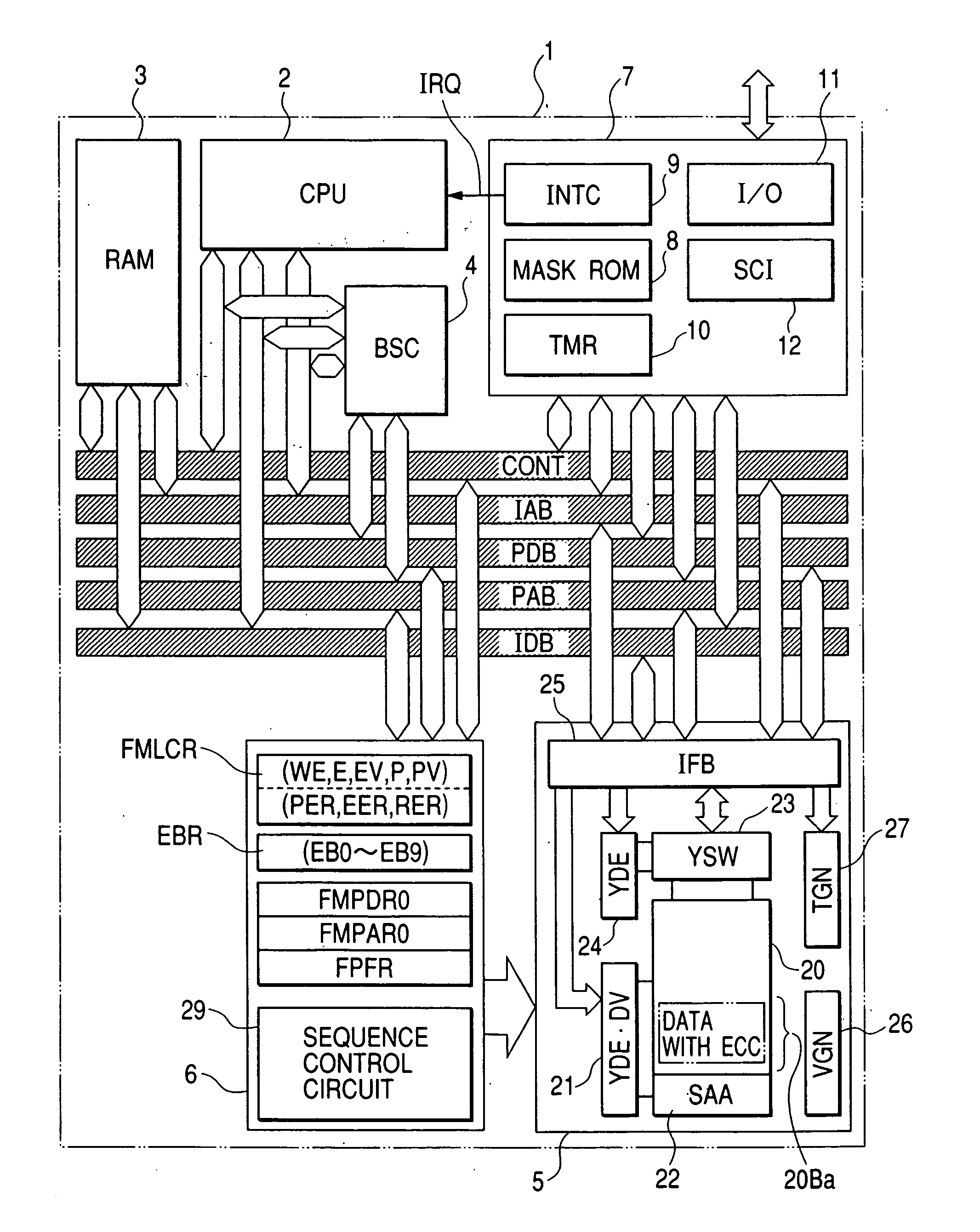
[0097]FIG. 1 shows a single-chip type microcomputer according to one embodiment of the present invention. Although not restricted in particular, the microcomputer 1 shown in the same drawing is formed on a single semiconductor substrate (semiconductor chip) by a CMOS integrated circuit manufacturing technology.

[0098] The microcomputer 1 includes a central processing unit (CPU) 2 used as an arithmetic control device or unit, a RAM 3, a bus state controller (BSC) 4, a flash memory 5 used as an electrically erasable and programmable non-volatile memory, a flash control module 6, and other module 7 which is a general term for other built-in circuits. The other module 7 include a mask ROM 8, an interrupt controller (INTC) 9, a timer (TMR) 10, an input / output port (I / O) 11 and a serial interface controller (SCI) 12, etc. These circuit modules are interfaced via buses IAB, IDB, PAB, PDB and CONT.

[0099] The buses IAB and IDB are respectively an internal address bus and an internal data b...

second embodiment

[0162]FIG. 31 shows a microcomputer corresponding to one example of a data processing system according to the present invention. The microcomputer 1 shown in the same drawing includes a flash memory 2 showing one example of an erasable and programmable non-volatile storage device, a CPU 3, a RAM (Random Access Memory) 4 and an interface circuit 5. They are connected to one another by an internal address bus 6, an internal data bus 7 and an unillustrated control data bus. The interface circuit 5 is connectable to an unillustrated peripheral circuit or the like via an external data bus 9 and an unillustrated external control bus. The microcomputer 1 shown in the same drawing is formed on a single semiconductor substrate or semiconductor chip such as monocrystal silicon or the like by, for example, a CMOS integrated circuit manufacturing technology.

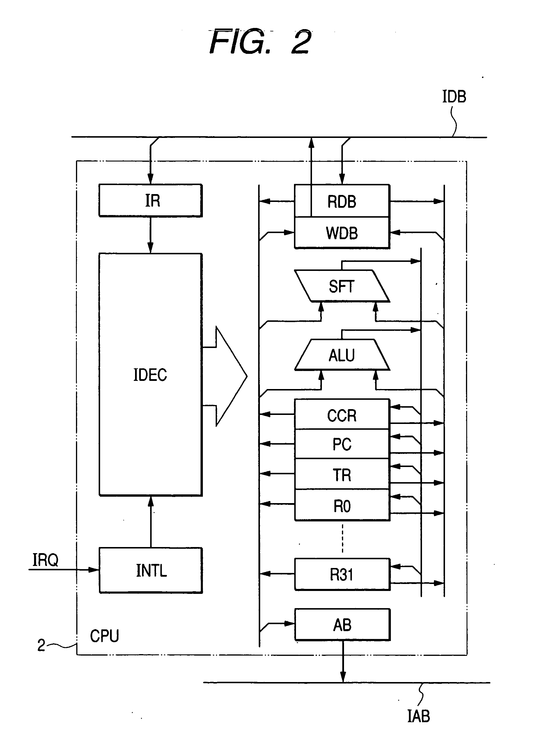
[0163] Although not shown in the drawing in particular, the CPU 3 has an instruction controller and an arithmetic unit. The instruction co...


PUM


Abstract

A data processing system (1) has an erasable and programmable non-volatile memory (5) and a central processing unit (2). The central processing unit allows only a specified partial storage area (20Ba) of the non-volatile memory to be intended for a software ECC process. Since ECC codes are added to the partial storage area alone and an error correction is made thereto to thereby increase the number of rewrite assurances, substantially needless waste of each storage area by ECC codes can b avoided as compared with a configuration in which the ECC codes are added to all the write data without distinction regardless of the storage areas. Further, since software copes with ECC processing, ECC correcting capability matched with a device characteristic of the non-volatile memory can easily be selected.

Description

BACKGROUND OF THE INVENTION [0001] The present invention relates to a technology for improving the number of rewrite assurances for a non-volatile memory, for example, a technology effective for application to a microcomputer with an electrically erasable and programmable flash memory built therein. [0002] An electrically erasable and programmable non-volatile memory (hereinafter also called simply “flash memory”) such as a flash memory or the like stores information according to the difference between threshold voltages programmed to memory cells. The difference between the threshold voltages is obtained according to the difference between the values or amounts of electrons or positive holes held in a floating gate. The performance of holding the electrons or positive holes in the flash memory is degraded with an increase in the number of rewritings. Accordingly, the number of rewrite assurances finite for the use of the flash memory is normally taken into consideration from the vi...

Claims


Application Information

Patent Timeline
Patent Type & Authority Applications(United States)
IPC IPC(8): G06F12/16G06F11/10G06F15/78G11C7/00G11C16/06G11C29/00
CPCG06F11/1068G06F12/16
Inventor YADA, NAOKIISHIKAWA, EIICHIHIRAKI, MITSURUSHUKURI, SHOJI
Owner RENESAS TECH CORP
Features
  • R&D
  • Intellectual Property
  • Life Sciences
  • Materials
  • Tech Scout
  • Unparalleled Data Quality
  • Higher Quality Content
  • 60% Fewer Hallucinations
Learn More