

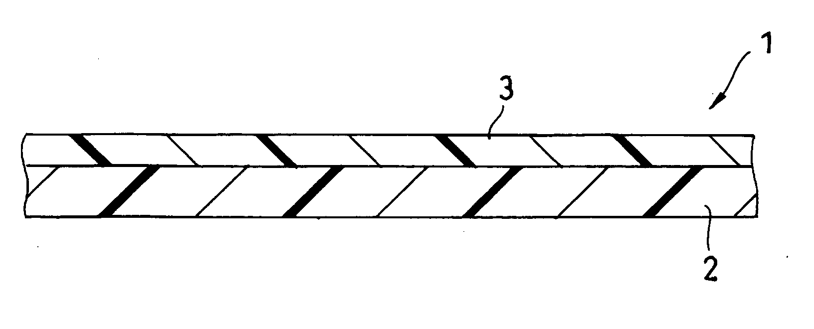
Sheet material and wiring board
a technology of wiring board and insulating layer, applied in the direction of printed circuit aspects, transportation and packaging, chemistry apparatus and processes, etc., can solve the problems of above-described conventional techniques, crack generation in the insulating layer of the wiring board, and addition of temperature change in the use environment to temperature change, so as to achieve excellent crack resistance and reliability.
- Summary
- Abstract
- Description
- Claims
- Application Information
AI Technical Summary
Benefits of technology
Problems solved by technology
Method used
Image

Examples
example 1
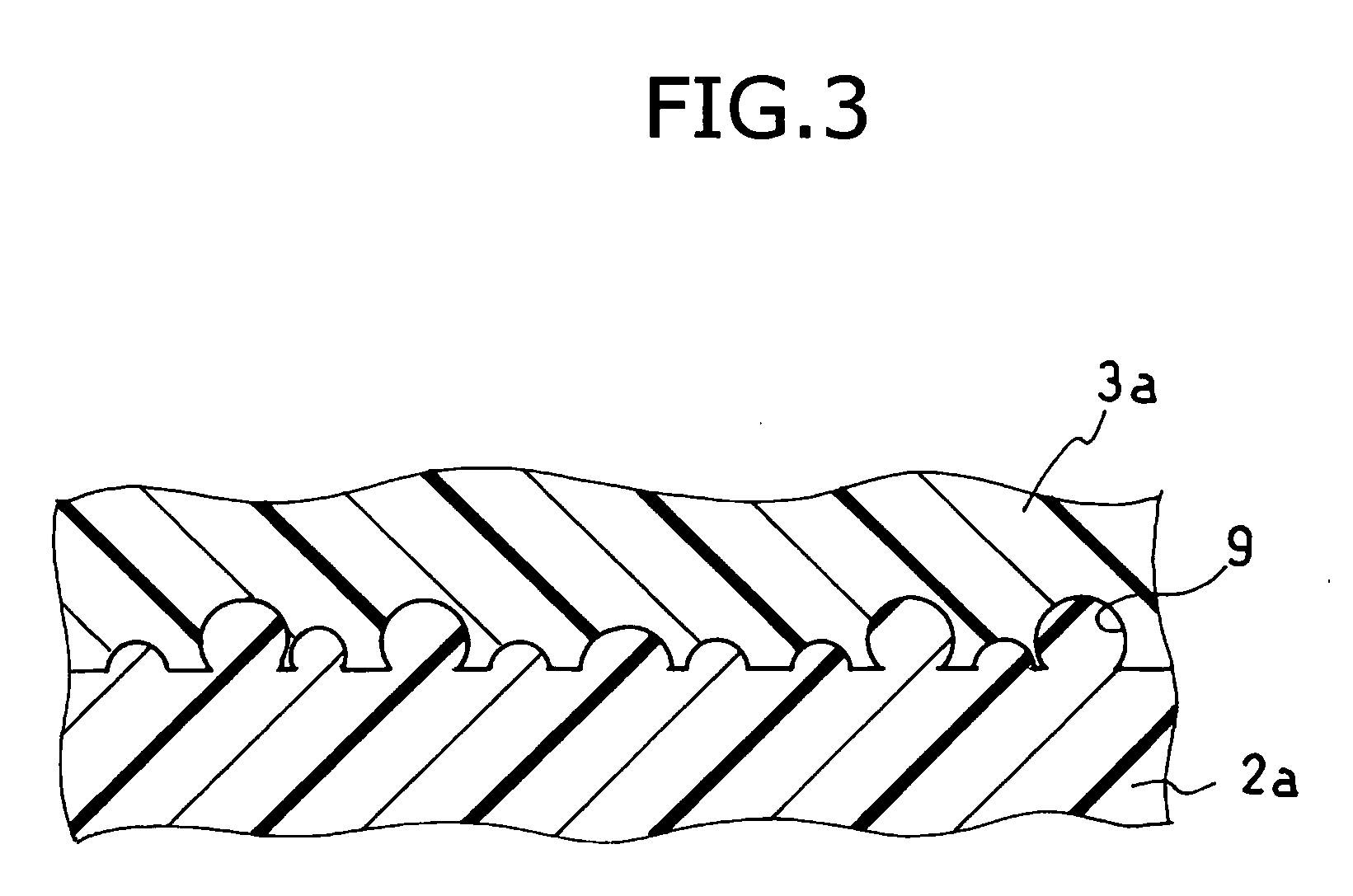
[0103] A double-sided copper clad polyimide film (UPISEL N fabricated by Ube Industries Ltd., a thickness of a copper foil: 12 μm, a thickness of polymide; 25 μm) was used. The copper foils on both sides of the double-sided copper clad polyimide film were dissolved with an alkali copper etchant when the surface of the polyimide film after etching the copper foils was observed with a scanning electron microscope (SEM), fine concave portions formed by transferring the mat faces of the copper foils were observed.
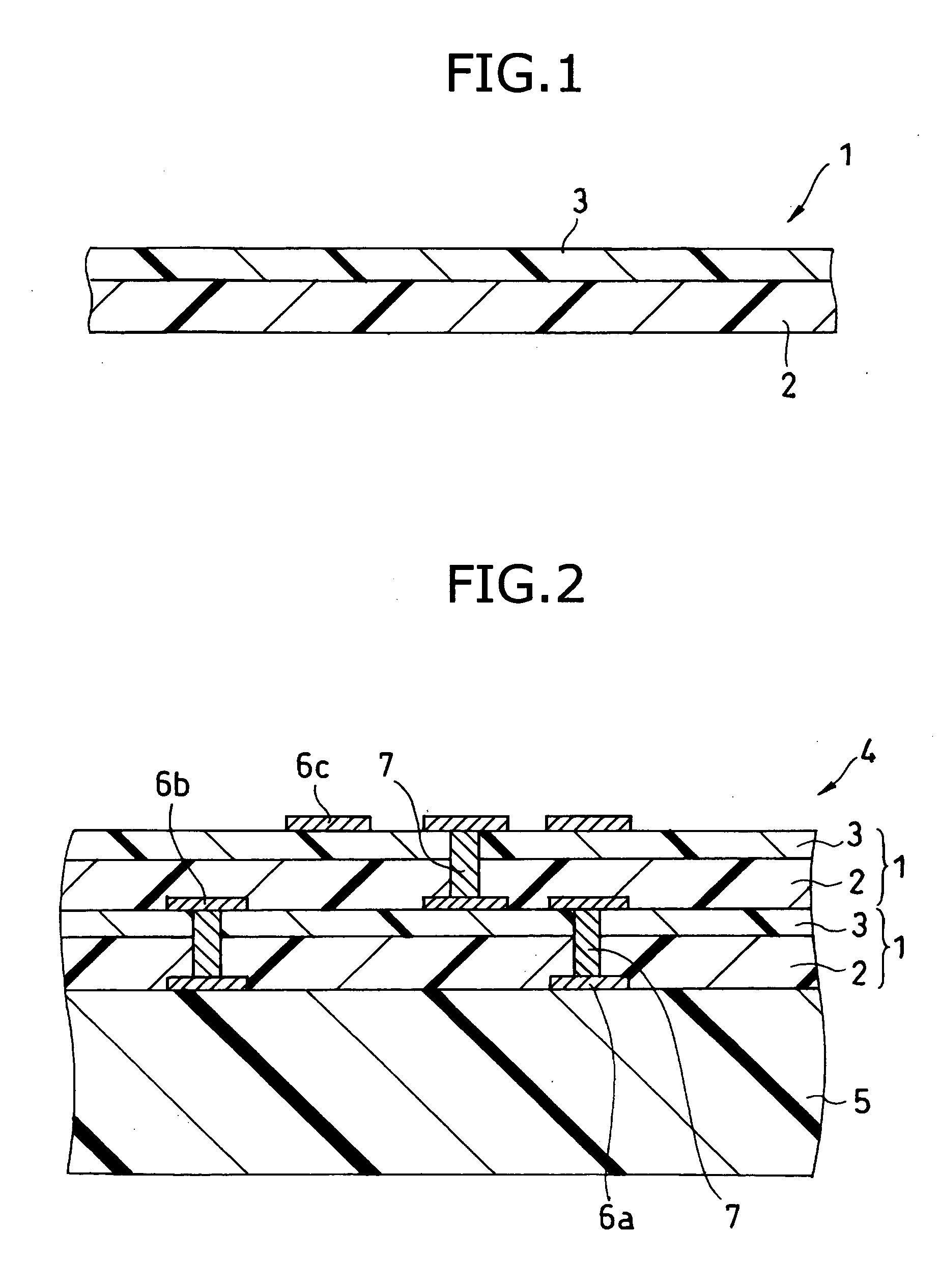
[0104] Next, the polyimide film, from which the copper foils were etched, and an epoxy resin material (ABF fabricated by Ajinomoto Co., Inc., a thickness: 40 μm) in a se-cured state (B-stage) were heated at 80° C. so as to be bonded to each other by a vacuum laminating technique, thereby obtaining a sheet material. On the other hand, an Ni-plating layer serving as an etching barrier layer was formed on a copper plate. On the thus formed etching barrier layer, a BGA land made o...
example 2
[0112] Only one side of a double-sided copper clad polyimide film was covered with a protective film so that only a copper foil on the other side was removed with the same etchant as that in Example 1. The thickness and the mechanical properties of the polyimide film were the same as those of the polyimide film in Example 1 described above. An epoxy resin (Probicote fabricated by Nippon Paint Co., Ltd., a thickness: 50 μm) in a semi-cured state was vacuum-laminated on the side of the polyimide film, from which the copper foil was etched away, thereby obtaining a laminate sheet material.
[0113] The laminate material war laminated and pressed on the same copper plate as that in Example 1 so as to obtain a sheet material formed on the copper plate. Next, the remaining copper foil was patterned so as to farm a wiring by a subtractive method. Next, after semiconductor elements were mounted, the copper plate was etched away to fabricate a wiring board.
[0114] As in Example 1, the epoxy re...
example 3
[0117] A laminate sheet material fabricated in the same manner as in Example 1 was laminated and pressed on an FR-4 substrate including a printed wiring. The laminated sheet material and the FR-4 substrate were kept at 170° C. for 80 minutes to cure a lower layer made of an epoxy resin included in the sheet material, thereby bonding the sheet material and the FR-4 substrate to each other. A part of the laminate material including the FR-4 substrate was cut out for the observation of its cross section. As a result, it was found that the epoxy resin layer protruded into the concave portions of the polyimide film. Although the polyimide layer and the epoxy resin layer were attempted to be separated from each other in this state, they could not be separated from each other because they were firmly bonded to each other.
[0118] After formation of a via in the sheet material on the FR-4 substrate by a laser, a desmear process was performed. Then, electroless plating using palladium as a ca...
PUM
| Property | Measurement | Unit |
|---|---|---|
| Temperature | aaaaa | aaaaa |
| Temperature | aaaaa | aaaaa |
| Temperature | aaaaa | aaaaa |
Abstract
Description
Claims
Application Information