Nitride and polysilicon interface with titanium layer

a polysilicon and titanium layer technology, applied in the direction of semiconductor devices, electrical devices, semiconductor/solid-state device details, etc., can solve the problems of low interface resistance, low resistance of the layer including the interface metal, and low nitrogen content, so as to reduce the resistance of the structure, fast destroy the barrier, and reduce the rate of any lateral oxidation.

Inactive Publication Date: 2006-01-05
INFINEON TECH AG +1
View PDF9 Cites 11 Cited by
  • Summary
  • Abstract
  • Description
  • Claims
  • Application Information

AI Technical Summary

Benefits of technology

[0046] The high temperature processing step also serves to anneal the other elements of the structure and to reduce the resistivity of the structure. For example, a structure incorporating a 1 nm titanium interface metal layer, a 16 nm tungsten nitride layer and a 40 nm tungsten conductor metal layer has a sheet resistance of about 10 ohms per square as deposited and about 4 to about 5 ohms per square after high temperature processing. The same structure has an interface resistance of about 70 Ω-μm2 after high temperature processing. By contrast, a comparable structure without the titanium layer has an interface resistivity of about 5,000-10,000 Ω-μm2 after high temperature processing.
[0047] A further advantage of structures according to preferred embodiments of the present invention is that such structures including the titanium interfacial metal are substantially stable when exposed to an oxidizing gas mixture of water vapor and hydrogen as, for example, exposure to such a mixture with respective relative mole fractions of 10% and 90% at an elevated temperature of above about 900° C.

Problems solved by technology

The layer including the interface metal, as deposited, desirably is relatively poor in nitrogen.
However, the structure, after high temperature processing, has an interface resistance substantially lower than a comparable structure with a metal nitride layer but without the interface metal.
It is believed that this, in turn, leads to a lower interface resistance than would occur in the ab

Method used


Image

  • Nitride and polysilicon interface with titanium layer
  • Nitride and polysilicon interface with titanium layer
  • Nitride and polysilicon interface with titanium layer

Examples


Embodiment Construction

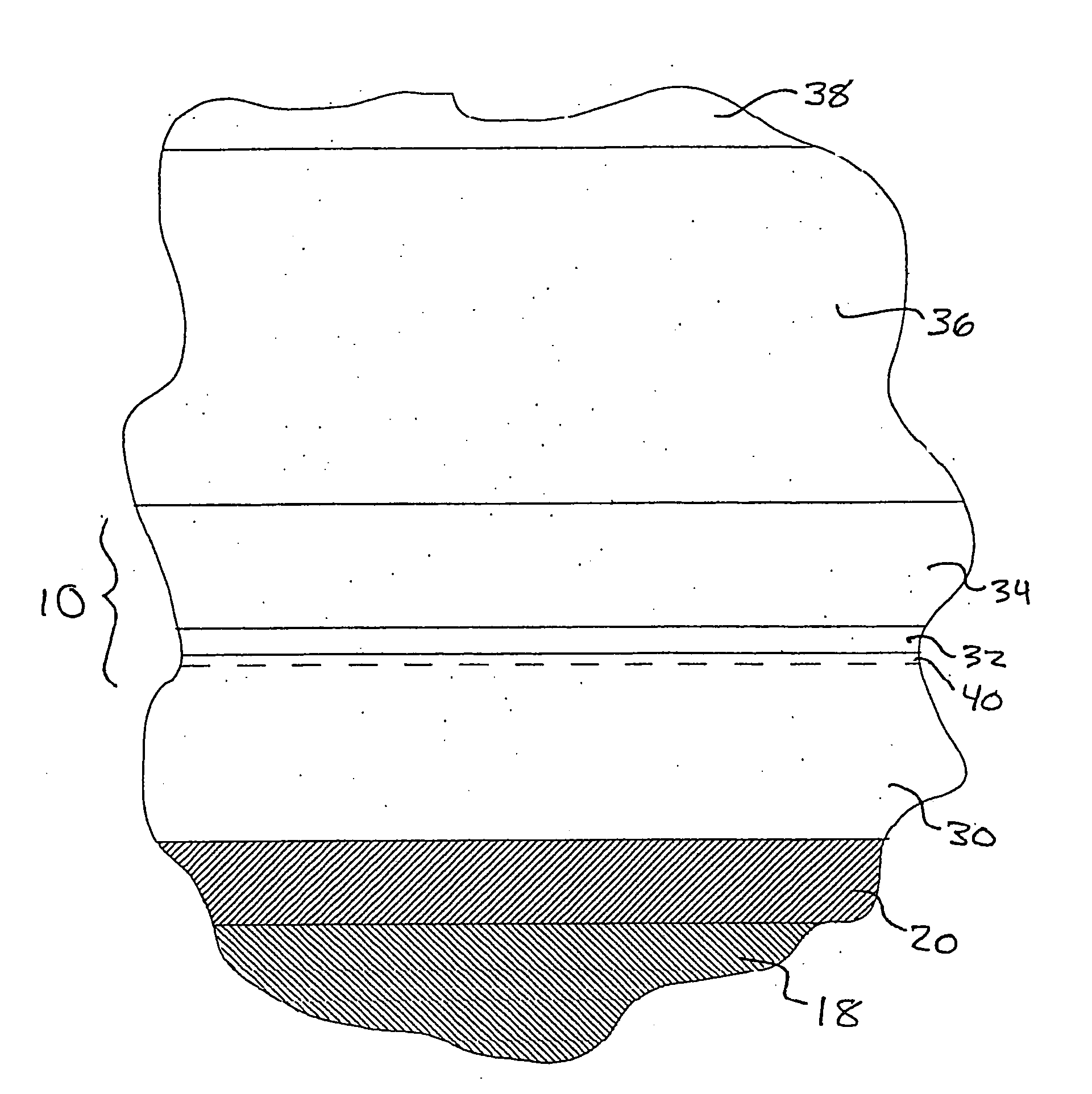
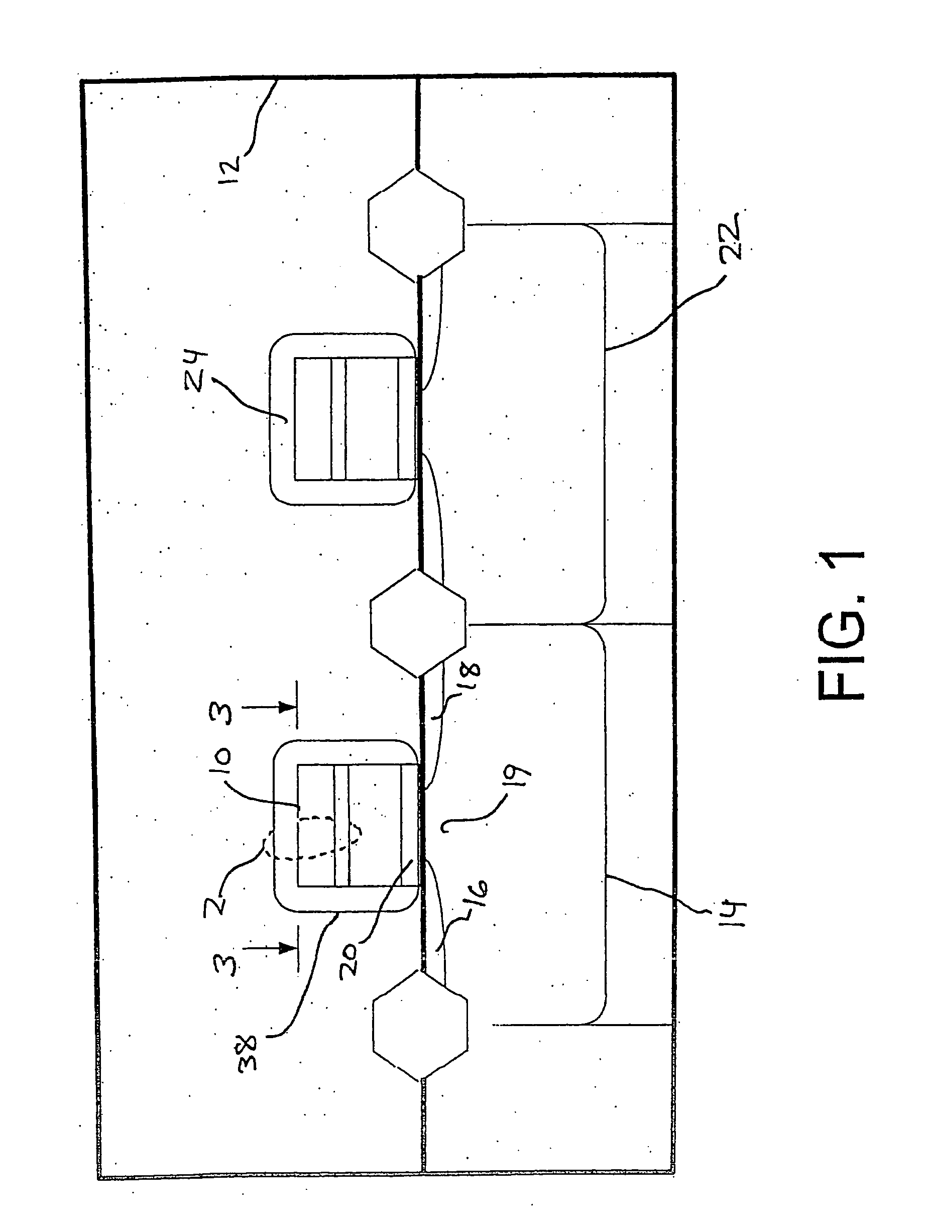
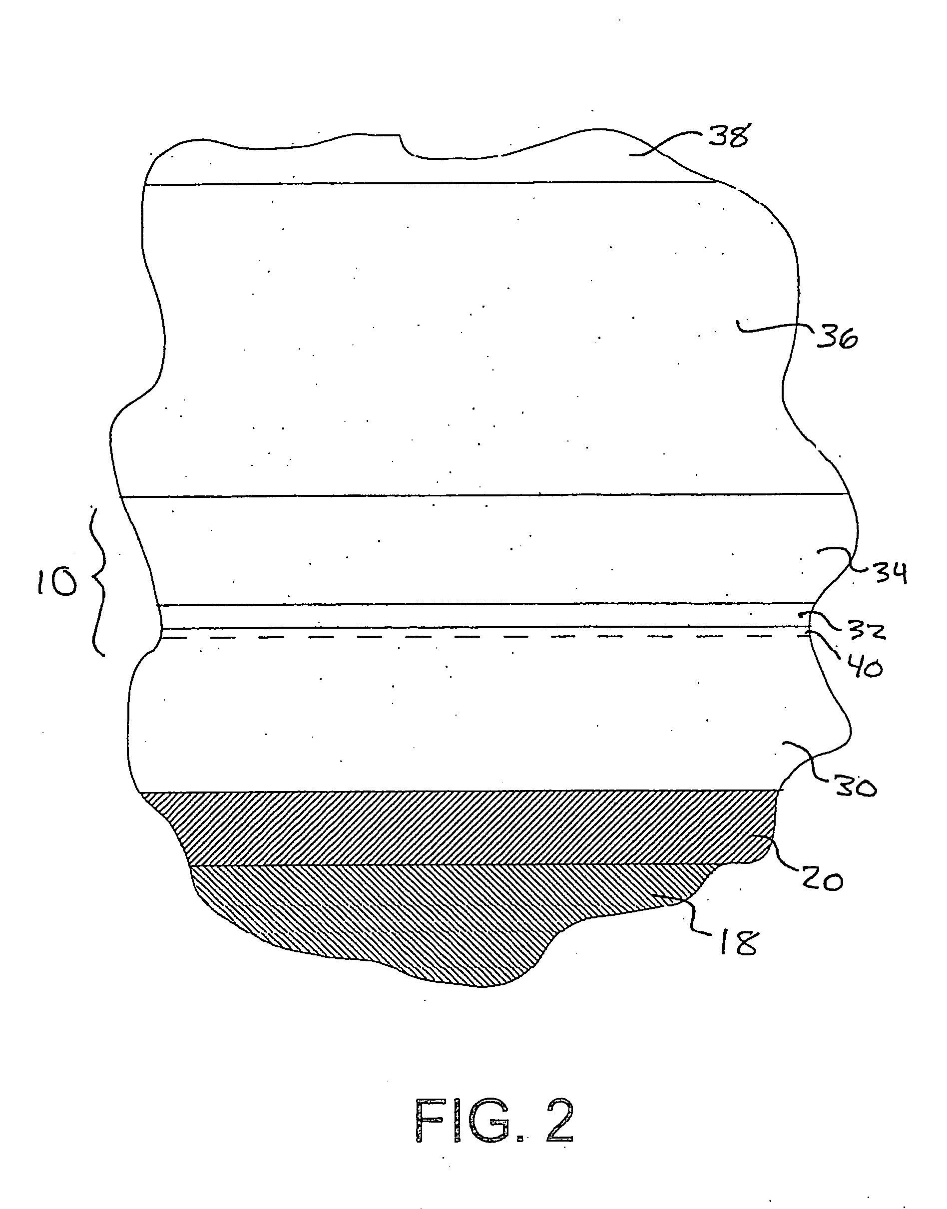
[0026] As depicted in FIG. 1, a conductive structure 10 according to one embodiment of the invention may be incorporated in an integrated circuit. Such a device may include large numbers of electronic elements in a unitary structure such as a chip or wafer. A small fragment of the unitary structure 12 is shown in FIG. 1. In the depicted structure, the conductive element 10 serves as the gate of a field effect transistor or FET 14. The FET includes a pair of n+-doped silicon regions 16 and 18, which serve as the source and drain of the FET, and a p-doped region 19 forming the channel. Conductive structure 10 is separated from the channel region 19 by an insulating layer 20. FET 14 may be part of a CMOS structure including a further FET 22 having opposite doping and associated with a further conductive element 24.

[0027] The gate insulator layer 20 can include various insulating materials such as silicon oxide, silicon oxynitride, silicon nitride, and so-called “high-k” insulators wit...


PUM


Abstract

A conductive structure in an integrated circuit (12), and a method of forming the structure, is provided that includes a polysilicon layer (30), a thin layer containing titanium over the polysilicon, a tungsten nitride layer (34) over the titanium-containing layer and a tungsten layer over the tungsten nitride layer. The structure also includes a silicon nitride interfacial region (38) between the polysilicon layer and the titanium-containing layer. The structure withstands high-temperature processing without substantial formation of metal silicides in the polysilicon layer (30) and the tungsten layer (32), and provides low interface resistance between the tungsten layer and the polysilicon layer.

Description

[0001] This application is a continuation of co-pending International Application No. PCT / US2003 / 029085, filed Sep. 16, 2003, which designated the United States and was published in English, and which claims priority to U.S. Provisional Patent Application No. 60 / 411,710, filed Sep. 18, 2002, both of which applications are incorporated herein by reference.TECHNICAL FIELD [0002] The present invention relates to conductive structures used in semiconductor devices and to methods of manufacturing the same. BACKGROUND [0003] Polycrystalline silicon or “polysilicon” structures are commonly used as conductive elements in integrated circuits. [0004] For example, in memories and other devices, an oxide-insulating layer overlies the channel region of a field effect transistor (“FET”) and a conductive polysilicon layer overlying the oxide layer serves as the gate of the FET. The amount of electrical charge on the gate controls the conductivity through the channel region of the FET. Thus, the sp...

Claims


Application Information

Patent Timeline
IPC IPC(8): H01L23/48H01L21/4763H01LH01L21/28H01L21/3205H01L21/336H01L21/768H01L23/522H01L29/40H01L29/51H01L29/78
CPCH01L21/28052H01L21/28061H01L21/76838H01L21/7685H01L21/76855H01L21/823828H01L2221/1078H01L29/4941H01L29/51H01L29/517H01L29/518H01L29/78H01L21/823842
Inventor SCHUTZ, RONALD J.ROBL, WERNERMALIK, RAJEEVCLEVENGER, LAWRENCE A.GLUSCHENKOV, OLEGCABRAL, CYRIL JR.IGGULDEN, ROY C.WANG, YUN-YUWONG, KEITH KWONG HONMCSTAY, IRENE LENNOX
Owner INFINEON TECH AG
Why Eureka
Try Eureka