Integrated circuit memory device and method

a memory device and integrated circuit technology, applied in the field of integrated circuits, can solve problems such as the need for refresh, and achieve the effect of high current gain and easy programing

Inactive Publication Date: 2006-01-05
MICRON TECH INC
View PDF84 Cites 37 Cited by
  • Summary
  • Abstract
  • Description
  • Claims
  • Application Information

AI Technical Summary

Benefits of technology

[0015] The above mentioned problems with DEAPROM memories and other problems are addressed by the present invention and will be understood by reading and studying the following specification. Systems and methods are provided for DEAPROM memories with metal oxide and / or low tunnel barrier interpoly insulators which require refresh. That is, the present invention describes the use of an ultra-thin metal oxide inter-poly dielectric insulators between the control gate and the floating gate to create a memory cell which has a high current gain, and is easy to program by tunneling but which requires refresh. The low barrier tunnel insulator between the floating gate and control gates makes erase of the cell easy but results in the requirement for refresh. These devices act like DRAM's and can be utilized as DRAM replacements. A coincident address is achieved by addressing both the control gate address lines (y-address) and source address lines α-address).

Problems solved by technology

The low barrier tunnel insulator between the floating gate and control gates makes erase of the cell easy but results in the requirement for refresh.

Method used


Image

  • Integrated circuit memory device and method
  • Integrated circuit memory device and method
  • Integrated circuit memory device and method

Examples


example i

Formation of Al2O3 or NiO Tunnel Barriers

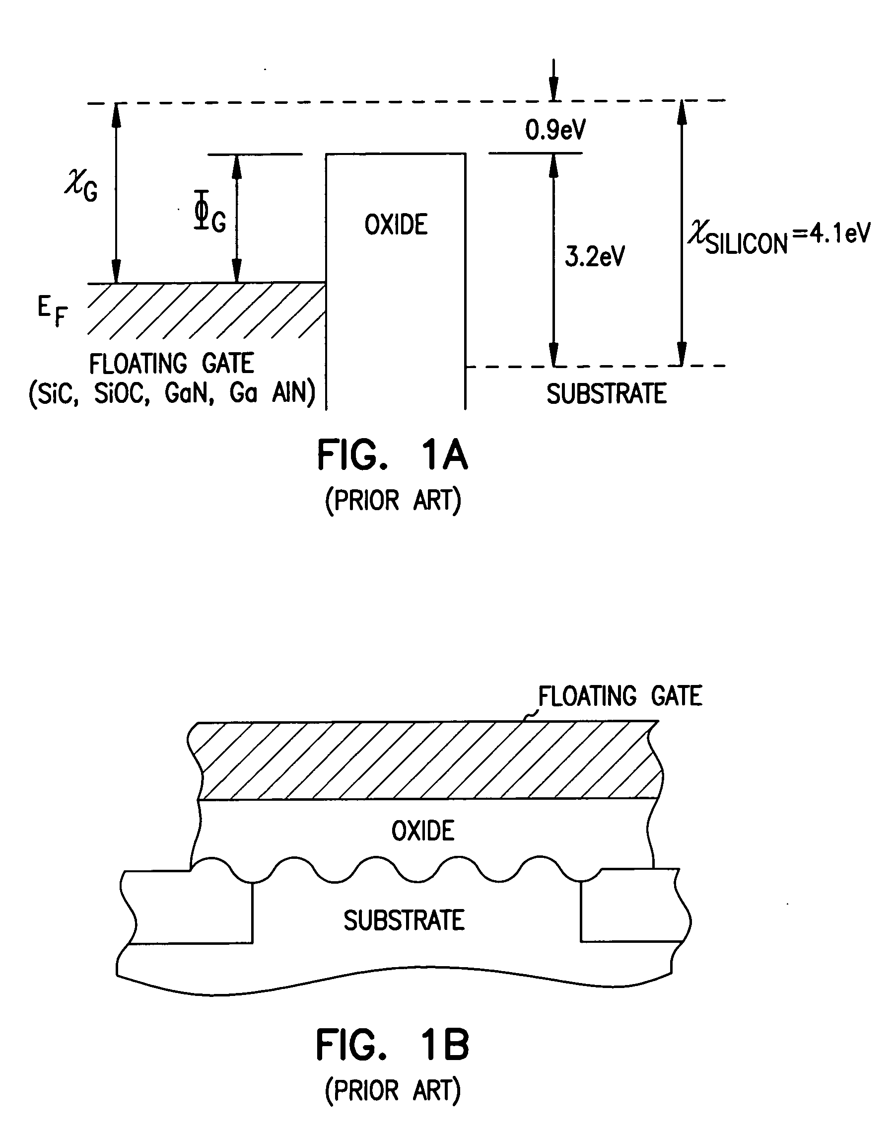
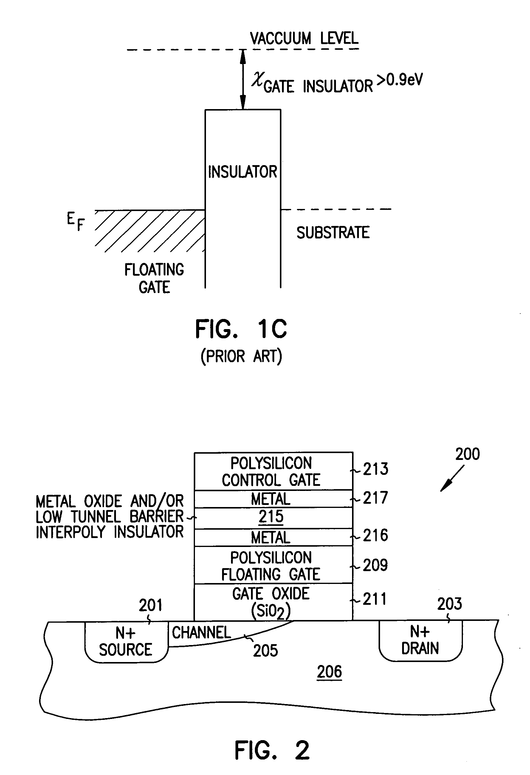
[0085] As stated above, the conventional large barrier insulating dielectrics are silicon oxide and silicon nitride. The realities are that silicon oxide is not an optimum choice for memory type devices, because the 3.2 eV tunnel barrier is too high resulting in premature failure of the insulators and limiting the number of operational cycles to be in the order of 105 to 107.

[0086] According to one embodiment of the present invention, a low tunneling barrier interpoly insulator is used instead, such as Al2O3 or NiO having a thickness of less than 20 Angstroms so that the tunneling barrier is less than 1.5 eV. A number of studies have dealt with electron tunneling in Al / Al2O3 / Al structures where the oxide was grown by “low temperature oxidation” in either molecular or plasma oxygen. Before sketching out a processing sequence for these tunnel barriers, note: [0087] (i) Capacitance and tunnel measurements indicate that the Al2O3 thickness incr...

example ii

Formation of Single- and Multi-Layer Transition Metal Oxide Tunnel Barriers

[0096] The band gap energies and barrier heights of some conventional gate insulators as silicon oxide, silicon nitride and aluminum oxide as well as tantalum oxide have been investigated and described in detail. Formation of single and double-layer dielectric layers of oxides of Ta2O5 and similar transition metal oxides can be accomplished by thermal as well as plasma oxidation of films of these metals.

[0097] In some cases the characteristics of the resulting dielectric insulators are not yet well known or well defined. Part of this detail is recounted as follows.

[0098] For example, single layers of Ta2O5, TiO2, ZrO2, Nb2O5 and similar transition metal oxides can be formed by “low temperature oxidation” of numerous Transition Metal (e.g., TM oxides) films in molecular and plasma oxygen and also by rf sputtering in an oxygen plasma. The thermal oxidation kinetics of these metals have been studied for decad...

example iii

Formation of Alternate Metal Compound Tunnel Barriers

[0107] Although no applications may be immediately obvious, it is conceivable that one might want to form a stack of oxide films having quite different properties, for example, a stack comprised of a high dielectric constant (k) oxide / a low k oxide / a high k oxide. “Low temperature oxidation” can be used to form numerous variations of such structures. While most of this disclosure deals with the formation and use of stacks of oxide dielectrics, it is also possible to use “low temperature oxidation” to form other thin film dielectrics such as nitrides, oxynitrides, etc. that could provide additional functions such as being altered by monochromatic light, etc. These will not be discussed further here.


PUM


Abstract

Structures and methods for DEAPROM memory with low tunnel barrier intergate insulators are provided. The DEAPROM memory includes a first source / drain region and a second source / drain region separated by a channel region in a substrate. A floating gate opposes the channel region and is separated therefrom by a gate oxide. A control gate opposes the floating gate. The control gate is separated from the floating gate by a low tunnel barrier intergate insulator having a tunnel barrier of less than 1.5 eV. The low tunnel barrier intergate insulator includes a metal oxide insulator selected from the group consisting of NiO, Al2O3, Ta2O5, TiO2, ZrO2, Nb2O5, Y2O3, Gd2O3, SrBi2Ta2O3, SrTiO3, PbTiO3, and PbZrO3. The floating gate includes a polysilicon floating gate having a metal layer formed thereon in contact with the low tunnel barrier intergate insulator. And, the control gate includes a polysilicon control gate having a metal layer formed thereon in contact with the low tunnel barrier intergate insulator.

Description

CROSS REFERENCE TO RELATED APPLICATIONS [0001] The present application is a divisional of U.S. application Ser. No. 10 / 789,038, filed on Feb. 27, 2004; which is a divisional of U.S. application Ser. No. 09 / 945,498, filed on Aug. 30, 2001, now issued as U.S. Pat. No. 6,778,441; each of which is incorporated herein by reference. [0002] This application is related to the following commonly assigned U.S. patent applications: “DRAM Cells with Repressed Memory Metal Oxide Tunnel Insulators,” Ser. No. 09 / 945,395, now issued as U.S. Pat. No. 6,754,108; “Programmable Array Logic or Memory Devices with Asymmetrical Tunnel Barriers,” Ser. No. 09 / 943,134; “Flash Memory with Low Tunnel Barrier Interpoly Insulators,” Ser. No. 09 / 945,507; “Field Programmable Logic Arrays with Metal Oxide and / or Low Tunnel Barrier Interpoly Insulators,” Ser. No. 09 / 945,512; “SRAM Cells with Repressed Floating Gate Memory, Metal Oxide Tunnel Interpoly Insulators,” Ser. No. 09 / 945,554; and “Programmable Memory Addres...

Claims


Application Information

Patent Timeline
Patent Type & Authority Applications(United States)
IPC IPC(8): G11C11/34G11C16/04H01L21/8247H01L27/115H01L29/51
CPCG11C16/0416H01L27/115H01L29/511H01L29/42324H01L29/51H01L27/11556H10B41/27H10B69/00
Inventor FORBES, LEONARDELDRIDGE, JEROME M.AHN, KIE Y.
Owner MICRON TECH INC
Why Eureka
Try Eureka