
Process for production of electroluminescent element and electroluminescent element

a technology of electroluminescent elements and electroluminescent elements, which is applied in the direction of photomechanical treatment originals, photomechanical instruments, instruments, etc., can solve the problems of disadvantageous removal of already formed organic el layers by solvents, low luminescence efficiency or service life, and few organic el materials can be rendered insoluble. , to achieve the effect of high production efficiency

Inactive Publication Date: 2006-01-12
DAI NIPPON PRINTING CO LTD
View PDF2 Cites 16 Cited by
  • Summary
  • Abstract
  • Description
  • Claims
  • Application Information

AI Technical Summary

Benefits of technology

[0025] In view of the above problems of the prior art, the present invention has been made, and an object of the present invention is to provide a production process of an electroluminescent element, which, while utilizing the advantages of photolithography, can prevent such an unfavorable phenomenon that the end part of the patterned part is eluted in a coating liquid coated after the formation of that part and, consequently, luminescent failure occurs as a result of cross contamination and a change in layer thickness and can realize high production efficiency, and to provide an electroluminescent element using the same.
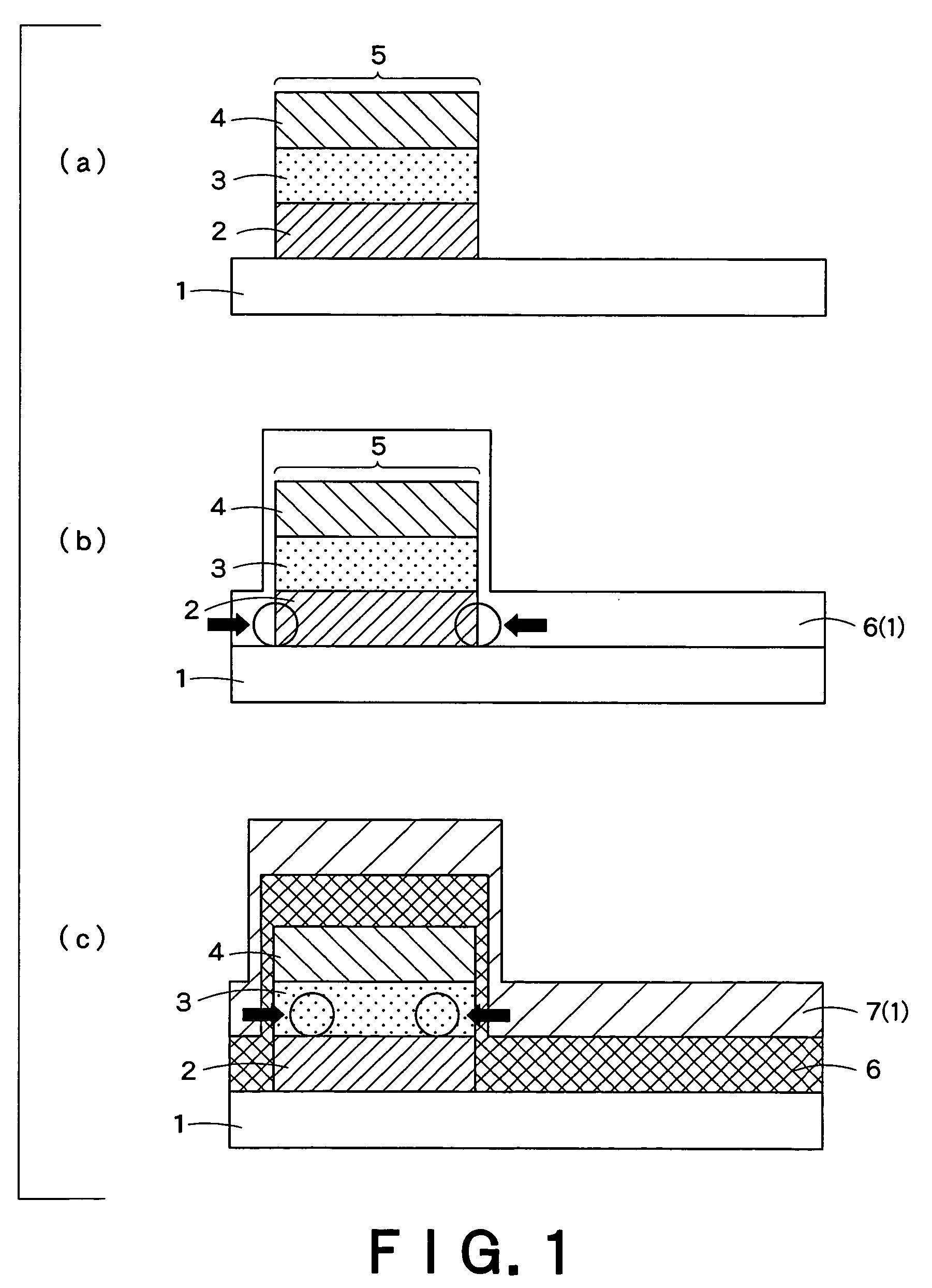
[0031] Further, even in the case where a luminescent layer is further provided on the buffer layer, the material for luminescent layer formation selected is generally a material of which the solubility is different from the material for buffer layer formation so that the material can be coated onto the buffer layer. Therefore, the end part of the already patterned first luminescent layer is not eluted in the solution for second buffer layer formation coated later, and, in addition, the coated second buffer layer functions as a protective layer, and, thus, elution of the end part of the first luminescent part in the solution for second luminescent layer formation coated later can be prevented.
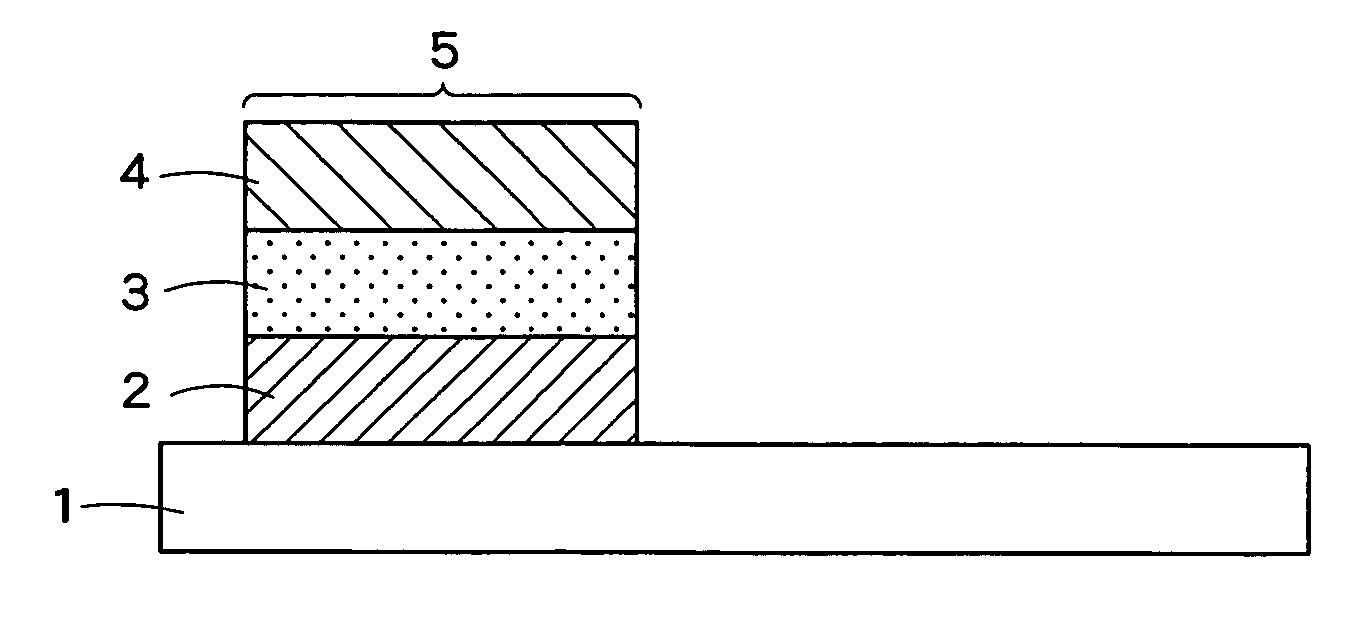
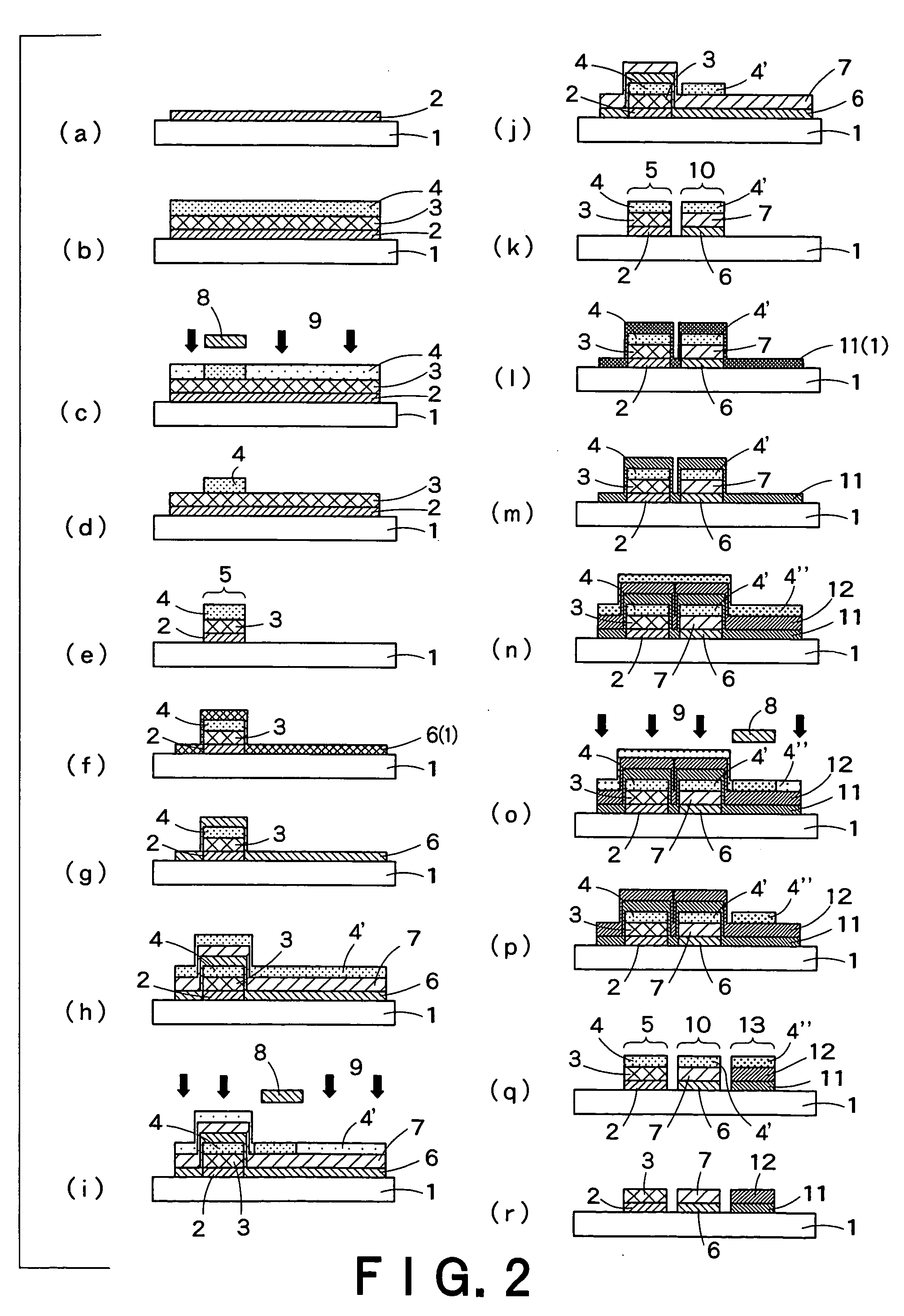
[0033] The production process of an electroluminescent element according to the present invention, as shown in FIG. 1, includes the step of forming a first pattern part 5 including a first buffer part 2 as the lowermost layer (FIG. 1 (a)) and the step of coating a solution 6 (1) for second buffer layer formation as the lowermost layer in a region including the first pattern part. In this process, a combination of the first buffer part with the solution for second buffer layer formation is such that the first buffer part is not miscible with the solution for second buffer layer formation. Therefore, in the first stage in the step of forming a second pattern part, when a solution 6 (1) for second buffer layer formation is coated in a region including the first pattern part 5 so as to form the lowermost layer, the end part of the already patterned first buffer part 2 is not eluted in the solution 6 (1) for second buffer layer formation coated later (FIG. 1 (b)). Further, even when a luminescent layer 3 is further provided, on the buffer layer 2, as an electroluminescent layer formed by photolithography, since the material for luminescent layer formation selected is generally a material having a solubility different from the material for buffer layer formation so that the material can be stacked onto the buffer layer by coating, the end part of the already patterned first luminescent part 3 is not eluted in the later coated solution 6 (1) for second buffer layer formation and, in addition, the coated and dried second buffer layer 6 functions as a protective layer, it is possible to prevent the end part of the first luminescent part from being eluted in the solution 7 (1) for second luminescent layer formation coated later (FIG. 1 (c)).
[0034] Likewise, even when a photoresist part 4 is further provided on the first buffer part, since the material for the photoresist layer is generally selected by taking into consideration the solubility so that the photoresist layer can be stacked by coating on the buffer layer, the end part of the already patterned first photoresist layer 4 is not eluted in the solution 6 (1) for second buffer layer formation coated later and, in addition, the coated second buffer layer 6 functions as a protective layer, it is possible to prevent the end part of the first photoresist layer 4 from being eluted in the solution for second photoresist layer formation coated later.
[0035] Accordingly, in the present invention, without the formation of a second photoresist layer (a protective layer) for covering the end part a of the patterned part as described in Japanese Patent Laid-Open No. 45656 / 2003, the occurrence of luminescence failure attributable to cross contamination or a change in layer thickness as a result of elution of the end of the patterned part in the coating solution coated after the formation of that part can be prevented. That is, in the present invention, an element, which comprises a plurality of types of high-definition pattern and exhibits good luminescence characteristics, can be prepared in a relatively easy and inexpensive manner.

Problems solved by technology

In general, however, among solvent-soluble organic EL materials used in the wet process, only a very few organic EL materials can be rendered insoluble in solvents by curing / crosslinking treatment.
Therefore, the wet process poses a problem that, in patterning organic EL materials different from each other in color on an identical substrate, the already formed organic EL layer is disadvantageously removed by the solvent.
In the above methods using a binder resin for fixing the organic EL material and the like, however, since the organic EL material is dispersed in the resin, the luminescence efficiency or the service life is disadvantageously lowered.
Therefore, in some cases, the properties of the organic EL material and the like are deteriorated by interaction between these impurities and the organic EL material.
In the above method, however, since the first luminescent part in its end part a and the second luminescent part in its end part b are exposed, in coating other coating liquid for a luminescent layer later, disadvantageously, the patterned luminescent part at its end part is eluted in the coating liquid for a luminescent layer which is coated later, and, consequently, cross contamination and a change in film thickness occurs, resulting in luminescence failure.
In the above method for forming a secondary photoresist layer (a protective layer) covering the end part a, the cross contamination and narrowing of pixels can be prevented, but on the other hand, the number of steps is large, posing a problem of production efficiency.

Method used


Image

  • Process for production of electroluminescent element and electroluminescent element
  • Process for production of electroluminescent element and electroluminescent element
  • Process for production of electroluminescent element and electroluminescent element

Examples


example 1

[0183] (Formation of First Buffer Layer)

[0184] A patterned ITO substrate having a size of 6 in. square and a thickness 1.1 mm was cleaned and was used as a base and a first electrode layer. A photocatalyst-containing solution for first buffer layer formation having the following composition was spin coated onto this substrate, and the coating was heated and dried at 150° C. for 10 min to allow hydrolysis and polycondensation to proceed and to cure the coating. Thus, a 200 angstrom-thick transparent photocatalyst-containing layer was formed in which a photocatalyst had been firmly fixed in organosiloxane.

[0185] (Composition of Solution for First Buffer Layer Formation)

Titanium dioxide (ST-K01, manufactured by2parts by massIshihara Sangyo Kaisha Ltd.)Organoalkoxysilane (TSL 8113, manufactured by0.4part by massToshiba Silicone Co., Ltd.)Fluoroalkylsilane (MF-160 E, manufactured0.3partby Tohchem Products Corporation) by massisopropyl alcohol3parts by mass

[0186] The buffer layer (pho...

example 2

[0201] (Formation of Buffer Layer)

[0202] Solid matter was separated from a dispersion of poly(styrenesulfonate) / poly(2,3-dihydrothieno[3,4-b]-1,4-dioxin (manufactured by Sigma-Aldrich Co.) in water by a supercentrifuge (Optima XL -100 K, manufactured by Beckman Coulter, Inc.) under conditions of 90,000 rpm×5 hr (20° C.), followed by filtration through a filter, predrying (150° C.×1 hr), grinding, and post-drying (under reduced pressure, 150° C.×12 hr) to give powder. A mixture of 100 parts by mass of the powder with 38 parts by mass of phosphorus pentaoxide was boiled under reflux at 170° C. for 10 hr and was distilled, followed by development in tetrahydrofuran. Insolubles were removed by filtration, 48 parts by mass of ethanol and 30 parts by mass of pyridine were added to the filtrate, and the mixture was stirred under reflux for 24 hr for esterification. After the completion of the esterification, the reaction mixture was filtered to remove insolubles, the solvent was removed f...

example 3

[0223] (Preparation of Solution for Buffer Layer Formation)

[0224]γ-Glycidoxypropyltrimethoxysilane having a glycido group (—CHOCH2) as a functional group (TSL 8350, manufactured by Toshiba Silicone Co., Ltd.) was added to an aqueous solution of PEDOT / PPS (Baytron P, manufactured by Bayer) represented by the above formula in proportions on a PEDOT / PPS solid basis as shown in Table 1 below to prepare a solution for buffer layer formation.

[0225] (Water Resistance Test)

[0226] The solution for buffer layer formation thus obtained was spin coated onto a glass substrate to form a 1000 angstrom-thick coating on a dry basis, and the coating was heat treated on a hot plate under conditions of 100° C.×10 min for crosslinking curing. Subsequently, the glass substrate with the coating formed thereon was immersed in 100 g of water to visually evaluate the state of coating.

[0227] (Measurement of Luminescence Efficiency)

[0228] Indium tin oxide (ITO) was vapor deposited onto a transparent glass...


PUM

PropertyMeasurementUnit
Percent by massaaaaaaaaaa
Fractionaaaaaaaaaa
Fractionaaaaaaaaaa

Abstract

There is provided a production process of an electroluminescent element, which, even when a buffer layer patterned by a photolithographic process is formed, luminescence failure derived from cross contamination or a variation in film thickness does not take place and can realize high production efficiency. The production process comprises repeating at least twice the step of forming an electroluminescent layer comprising a buffer layer and a luminescent layer by patterning using a photolithographic process, thereby producing an electroluminescent element comprising a patterned electroluminescent layer, and comprises the steps of forming a first pattern part comprising a first buffer layer as the lowermost layer; and coating a solution for second buffer layer formation in a region including said first pattern part, the first buffer layer being immiscible with said solution for second buffer layer formation.

Description

BACKGROUND OF THE INVENTION [0001] 1. Field of the Invention [0002] The present invention relates to a process for producing an electroluminescent (hereinafter often abbreviated to “EL”) element comprising an electroluminescent layer formed by photolithography, and an electro-luminescent element. [0003] 2. Background Art [0004] EL elements cause holes and electrons, injected from opposed electrodes, to be combined within a luminescent layer to emit energy which excites a fluorescent material within the luminescent layer to emit light of a color corresponding to the fluorescent material, and have drawn attention as selfluminous planar display elements. [0005] Among others, organic thin-film EL displays using an organic material as a luminescent material are expected to be applied to advertising or other low-cost simple displays that have high luminescence efficiency, for example, can realize high-brightness luminescence even in an applied voltage of a little less than 10 V, can emit ...

Claims


Application Information

Patent Timeline
IPC IPC(8): G03C5/00H01L27/32H01L51/00H01L51/56
CPCH01L27/3211H01L51/56H01L51/0037H01L51/0018H10K59/35H10K71/233H10K85/1135H10K71/40H10K71/00
Inventor ITOH, NORIHITOTACHIKAWA, TOMOYUKIITOH, KIYOSHI
Owner DAI NIPPON PRINTING CO LTD
Learn More