Wiring pattern and method of manufacturing the same and thin film magnetic head and method of manufacturing the same

a manufacturing method and wiring pattern technology, applied in the direction of metal sheet head, superimposed coating process, instruments, etc., can solve the problems of insufficiently large magnetic flux, inability to form submicron pattern precisely, and inability to generate sufficient magnetic flux for recording stably, etc., to avoid deterioration of magnetic materials, excellent electrical insulation property, and superior step-coverage

Inactive Publication Date: 2006-01-19
HEADWAY TECH INC +1
View PDF5 Cites 8 Cited by
  • Summary
  • Abstract
  • Description
  • Claims
  • Application Information

AI Technical Summary

Benefits of technology

[0036] It is another object of the present invention to provide a thin film magnetic head and a combination type thin film magnetic head, in which a coil width LC is shortened by decreasing a space between successive coil windings and a magnetic path length LM is shortened to improve a performance of the head.
[0037] It is further object of the invention to provide a method of manufacturing easily and precisely a thin film magnetic head and a combination type thin film magnetic head, in which a coil width LC is shortened by decreasing a space between successive coil windings and a magnetic path length LM is shortened to improve a performance of the head.
[0085] As explained above, in the thin film magnetic head according to the invention, since the thin film coil is formed by the first and second thin film coil halves and spaces between successive coil windings of the first thin film coil half are set to a value slightly larger than a width of the coil windings, successive coil windings of the second thin film coil half can be formed in these spaces in a self-aligned manner. Therefore, distances between successive coil windings of the first and second thin film coil halves can be extremely shortened and a magnetic path length can be shortened. Then, characteristics such as the flux rise time property, NLTS property and over write property can be improved.
[0086] In the thin film magnetic head according to the invention, a space between successive coil windings of the first and second thin film coil halves may be preferably not larger than 0.2 μm, and more particularly may be preferably set to a value within a range of 0.03-0.15 μm. If a space between successive coil windings is smaller than 0.03 μm, the coil windings could not be isolated well. If a space between successive coil windings is larger than 0.2 μm, a magnetic path length of the thin film magnetic head could not be shortened effectively. As explained above, according to the present invention, by reducing a space between successive coil windings to not larger than 0.2 μm, particularly to a value within a range of 0.03-0.15 μm, a magnetic path length can be shortened less than a half of the conventional thin film magnetic head illustrated in FIG. 9 without decreasing a width of coil windings. According to the invention, a magnetic path length can be shorter than that of the inductive type thin film magnetic heads disclosed in the above mentioned U.S. Pat. Nos. 6,191,916 and 6,204,997. In this manner, the performance of the thin film magnetic head can be improved to a large extent.
[0109] In the method of manufacturing a thin film magnetic head according to the invention, it is preferable that said first insulating film for isolating the first and second thin film coil halves may be preferably formed by alumina-CVD. The alumina-CVD may be preferably a reduced pressure Al2O3—CVD film formed by an atomic layer process, in which AlCl3 and H2O, N2, N2O or H2O2 are alternately projected intermittently under a reduced pressure of 1-2 Torr at a temperature of 100-400° C., preferably 150-200° C. In order to avoid a deterioration of magnetic materials by a heating process, it is preferable that a heating temperature is not higher than 300° C. However, if a heating time is short, a higher temperature of, for instance 400° C. does not cause a serious problem. In this manner, it is possible to obtain the insulating film which has an excellent electrically insulating property as well as a superior step-coverage although the insulating film has a large thickness.

Problems solved by technology

However, upon decreasing a track width by utilizing the semiconductor manufacturing process, there is a problem that a sufficiently large magnetic flux could not be obtained due to a miniaturized structure of the pole portion.
However, when a width of the track pole is reduced to sub-micron order, such magnetic materials could not generate a sufficiently large magnetic flux for recording stably.
Therefore, it is quite difficult to form the pattern of submicron order precisely.
However, these magnetic materials could not be easily formed by sputtering into a film having a given pattern.
However, etching rate is too slow and a track width of submicron order could not be controlled precisely.
It would be possible to shorten the magnetic path length by reducing a pitch of successive coil windings of the thin film coil, but this solution has a limitation.
Therefore, when the seed layer is etched by the ion milling, a portion of the seed layer hidden by the inclined portion could not be removed sufficiently and coil windings might be short-circuited.
In this manner, in the known thin film magnetic head, a magnetic path length could not be shortened, and a high frequency property could not be improved.
In the known combination type thin film magnetic head explained above, there is a problem of miniaturizing the writing inductive type thin film magnetic head element.
However, in order to reduce an electric resistance of the thin film coil, a width of coil winding should be shortened only with a limitation.
Furthermore, the bottom pole 10 and top pole 21 are also heated to expand and a serious problem of pole protrusion might occur and the thin film magnetic head might be brought into contact with the record medium.
However, this result in a re-deposition of debris of the seed material and successive coil windings might not be separated well, and thus a distance between successive coil windings could not be shortened.
If a distance between successive coil windings is shortened less than the above value, the above mentioned problem might occur.
If a width of a wall defining the opening in the photoresist film is shorted in order to shorten a distance between successive coil windings, the thin wall might be broken due to the stirring of the plating liquid.
Then, the thin film coil could not be formed accurately.
However, then an apex angle might be increased and a narrow track width could not be attained.
Then, the number of coil windings could not be increased and the NLTS property could not be improved.
Such etching debris might short-circuit the coil windings.
However, since use is made of the photoresist film having a given patter of openings for forming the second thin film coil half, the first and second thin film coil halves could not be formed in a self-aligned manner.
Therefore, it is difficult to shorten a space between successive coil windings in the order of quartermicrons.
The above explained problems occur not only in the thin film magnetic head, but also in case of forming fine conductive patterns in the semiconductor integrated circuits.
However, the known manufacturing methods suitable for a mass production could not satisfy such a requirement.
However, such a structure of conductive pattern could not be manufactured by the conventional methods.

Method used


Image

  • Wiring pattern and method of manufacturing the same and thin film magnetic head and method of manufacturing the same
  • Wiring pattern and method of manufacturing the same and thin film magnetic head and method of manufacturing the same
  • Wiring pattern and method of manufacturing the same and thin film magnetic head and method of manufacturing the same

Examples


Embodiment Construction

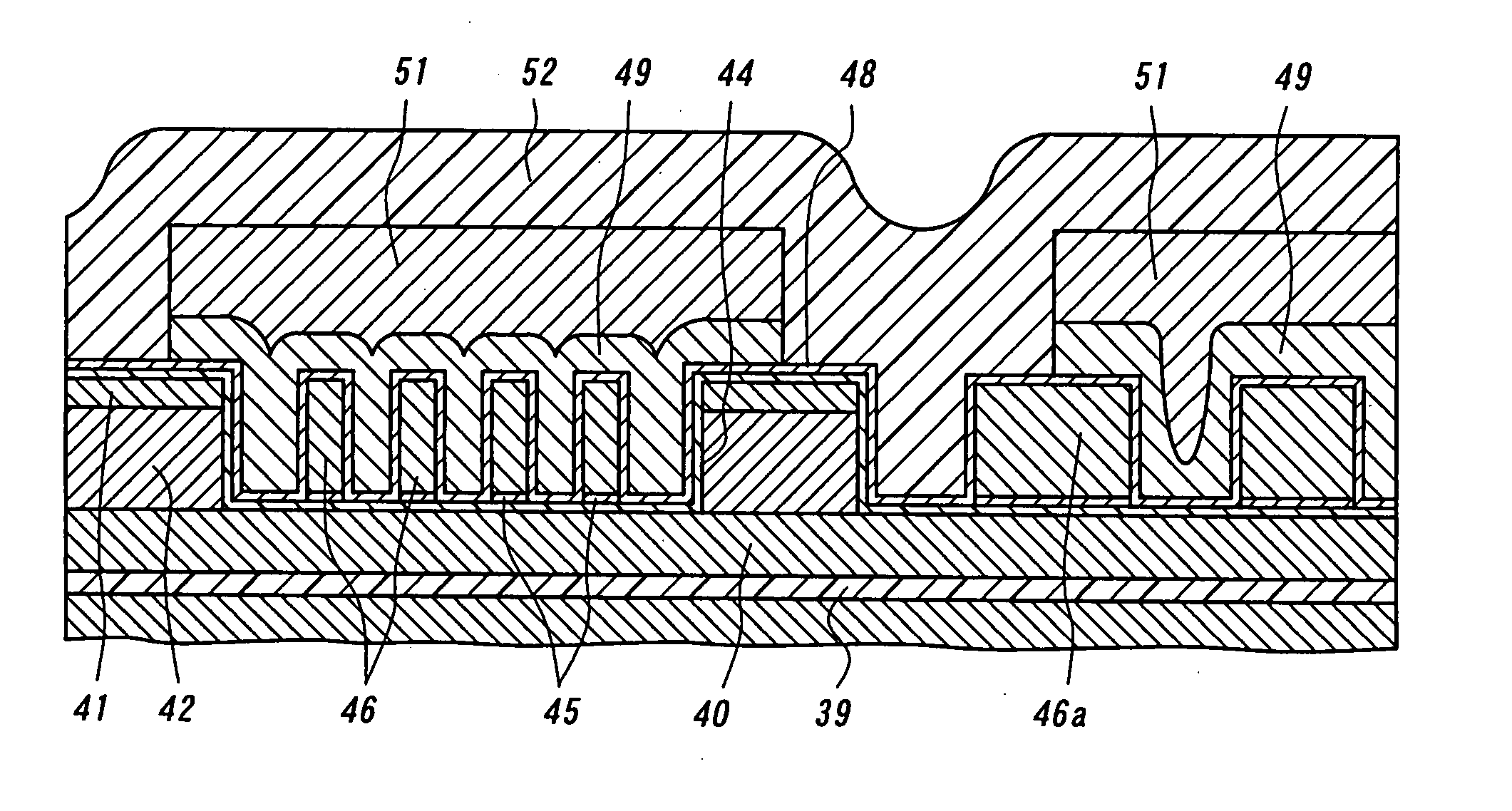
[0119]FIGS. 10-22 are cross sectional and plan views showing successive steps of the method of manufacturing a first embodiment of the combination type thin film magnetic head according to the invention. In these drawings, A denotes a cross sectional view cut along a line perpendicular to the air bearing surface, and B represents a cross sectional view of a pole portion cut along a line parallel to the air bearing surface. It should be noted that the structure of a reading GMR head element formed by a magnetoresistive type thin film magnetic head and the method of manufacturing the same are substantially identical with those of the known head. As illustrated in FIGS. 10A and 10B, an insulating film 32 made of alumina and having a thickness of about 3 μm is deposited on one surface of a substrate 31 made of AlTiC. Furthermore, a bottom shield film 33 made of a permalloy for the magnetoresistive type thin film magnetic head is formed on the insulating film with a thickness of about 2-...


PUM

PropertyMeasurementUnit
temperatureaaaaaaaaaa
saturation magnetic flux densityaaaaaaaaaa

Abstract

A bottom track pole is formed on a surface of a bottom pole, a thin film coil is formed on the bottom pole to form a flat coplanar surface with the bottom track pole, a write gap film is formed on the flat coplanar surface, first and second magnetic material films constituting a top pole are formed on a flat surface of the thin film coil, and the second magnetic material film, first magnetic material film, write gap film and bottom track pole are partially removed by RIE to form a top track pole and trim structure in a self-aligned manner. The thin film coil is formed by a first thin film coil half and a second thin film coil half having coil windings which are formed in a self-aligned manner between successive coil windings of the first thin film coil half and have a two-layer structure of a first conductive film at least a part of which is formed by CVD and a second conductive film formed by electrolytic plating. A thin insulating film is interposed between successive coil windings of the first and second thin film coil halves. Jumper wirings for connecting an innermost coil winding of the first thin film coil half to an outermost coil winding of the second thin film coil half are formed together with the top pole.

Description

[0001] This is a Division of application Ser. No. 10 / 067,863 filed Feb. 8, 2002. The entire disclosure of the prior application is hereby incorporated by reference herein in its entirety.BACKGROUND OF THE INVENTION [0002] 1. Field of the Invention [0003] The present invention generally relates to an electrically conductive wiring pattern and a method of manufacturing the same, and also relates to a thin film magnetic head comprising a thin film coil formed by a wiring patter, The present invention also relates to a combination type thin film magnetic head having an inductive type writing thin film magnetic head element and a magnetoresistive type reading thin film magnetic head element stacked one on the other, and a method of manufacturing the same. More particularly, the present invention relates to a combination type thin film magnetic head and a method of manufacturing the same, in which a GMR element is used as a magnetoresistive type thin film magnetic head element and an indu...

Claims


Application Information

Patent Timeline
Patent Type & Authority Applications(United States)
IPC IPC(8): G11B5/147G11B5/17G11B5/31G11B5/39H01F17/00H01F41/04
CPCG11B5/17Y10T29/49062G11B5/313G11B5/3136G11B5/3163G11B5/3967H01F17/0013H01F41/042Y10T29/49043Y10T29/49046Y10T29/49044Y10T29/49034Y10T29/49052Y10T29/49048Y10T29/4906Y10T29/49064G11B5/3109
Inventor SASAKI, YOSHITAKAKAMIGAMA, TAKEHIRO
Owner HEADWAY TECH INC
Why Eureka
Try Eureka