Semiconductor-ferroelectric storage device and its manufacturing method

a technology of ferroelectric storage and semiconductors, applied in vacuum evaporation coatings, chemical vapor deposition coatings, coatings, etc., can solve the problem of inability to control the electrical conduction between the source and drain of the transistor, the electric polarization of the ferroelectric, etc., to improve crystallinity and ferroelectricity, reduce leakage current, and improve the effect of temperatur

Active Publication Date: 2006-01-26
NAT INST OF ADVANCED IND SCI & TECH
View PDF6 Cites 18 Cited by
  • Summary
  • Abstract
  • Description
  • Claims
  • Application Information

AI Technical Summary

Benefits of technology

[0044] Data storage is based on the electric polarization of the ferroelectric film 3. In order to have ferroelectricity, the ferroelectric film 3 should be heated to a high temperature, during the thin-film formation or in a subsequent heat treatment, to thereby bring the film 3 into a crystalline state. This crystallization temperature is generally from 650° C. to 950° C. In general, the higher the temperature, the better the crystallinity and ferroelectricity. The period of the crystallization step is typically 1 hour. For forming a source region and a drain region in the silicon, a short-time (typically 30 seconds) heat treatment at a temperature of at least about 1050° C. is necessary for activation of the impurities. The insulator buffer layer 2 inevitably undergoes this high-temperature step for crystallizing the ferroelectric film 3. In a standard production process, the buffer layer 2 further undergoes a heat treatment step for forming a source region and a drain region. Accordingly, in processes heretofore, the insulator buffer layer 2 is also disadvantageously crystallized in the heat treatment step and this has resulted in leakage current flowing through grain boundaries between crystal grains. In the case of the HfO2+u or Hf1−xAl2xO2+x+y in this embodiment, the insulator buffer layer 2 is not crystallized but retains the amorphous state even in the thermal step for ferroelectric crystallization or in the thermal step for activation of the impurities. Consequently, the insulator buffer layer 2 can have a reduced leakage current. The surface of the insulator buffer layer 2 in an amorphous state is smoother than the insulator buffer layer which has been crystallized. Seed crystals for the growth of crystals of a ferroelectric film 3 are less apt to generate from the surface of the amorphous insulator buffer layer 2. Accordingly, crystal grains of ferroelectric film 3 can be small, dense thin film can be formed, and the leakage current flowing through the ferroelectric film 3 can be reduced. On the other hand, when the insulator buffer layer 2 is crystallized, this layer has enhanced surface irregularities due to the crystal grains and grain boundaries. These crystal grains are apt to generate seed crystals for a ferroelectric film 3, and the resultant ferroelectric film 3 is constituted of large crystal grains and has an increased leakage current. As described above, by constituting an insulator buffer layer 2 of HfO2+u or Hf1−xAl2xO2+x+y the leakage current flowing through each of the insulator buffer layer 2 and the ferroelectric film 3 can be reduced and a memory transistor having a truly sufficient long data holding time is realized. Hf1−xAl2xO2+x+y retains its amorphous state at even higher temperatures than HfO2+u in a heat treatment step and, hence, is especially preferred when a ferroelectric having a high crystallization temperature is used as the ferroelectric film 3.
[0045] Production processes are explained next. It is a matter of course that the production processes of the present invention should not be construed as being limited to the following processes.
[0046] For forming the insulator buffer layer 2, any technique for thin-film formation can be used. Effective techniques for physical vapor deposition include pulsed-laser deposition (also called laser ablation), sputtering, and vapor deposition. Examples of chemical deposition include MOCVD (metal organic chemical vapor deposition), MOD (metal organic decomposition), and a sol-gel method.
[0047] For forming the ferroelectric film 3 and the gate electrode 4 also, any technique for thin-film formation can be used. Effective techniques for physical vapor deposition include pulsed-laser deposition, sputtering, and vapor deposition. Examples of chemical deposition include MOCVD, MOD, and a sol-gel method.
[0048] An example of production processes is explained below in which silicon is used as a semiconductor substrate 1 and pulsed-laser deposition is used for forming an insulator buffer layer 2 and a ferroelectric film 3.
[0049] A silicon surface is cleaned by a standard surface-cleaning method. Thereafter, the oxide layer remaining on the surface is removed with dilute hydrofluoric acid or buffered hydrofluoric acid. Furthermore, a surface treatment for, e.g., purposely forming an oxide film, nitride film, or oxynitride film composed of from one to several molecular layers may be conducted.

Problems solved by technology

This is mainly because the buffer layer and the ferroelectric have a high leakage current and, hence, charge is accumulated around the interface between the ferroelectric and the buffer layer, and this charge shields the electric polarization in the ferroelectric, making it impossible for the electric polarization of the ferroelectric to control electrical conduction between the source and drain in the transistor.
Furthermore, there is a problem that although a voltage is applied to the MFIS in data writing in the ferroelectric, most of the voltage acts on the buffer layer when the buffer layer has a low dielectric constant.

Method used


Image

  • Semiconductor-ferroelectric storage device and its manufacturing method
  • Semiconductor-ferroelectric storage device and its manufacturing method
  • Semiconductor-ferroelectric storage device and its manufacturing method

Examples


example 1

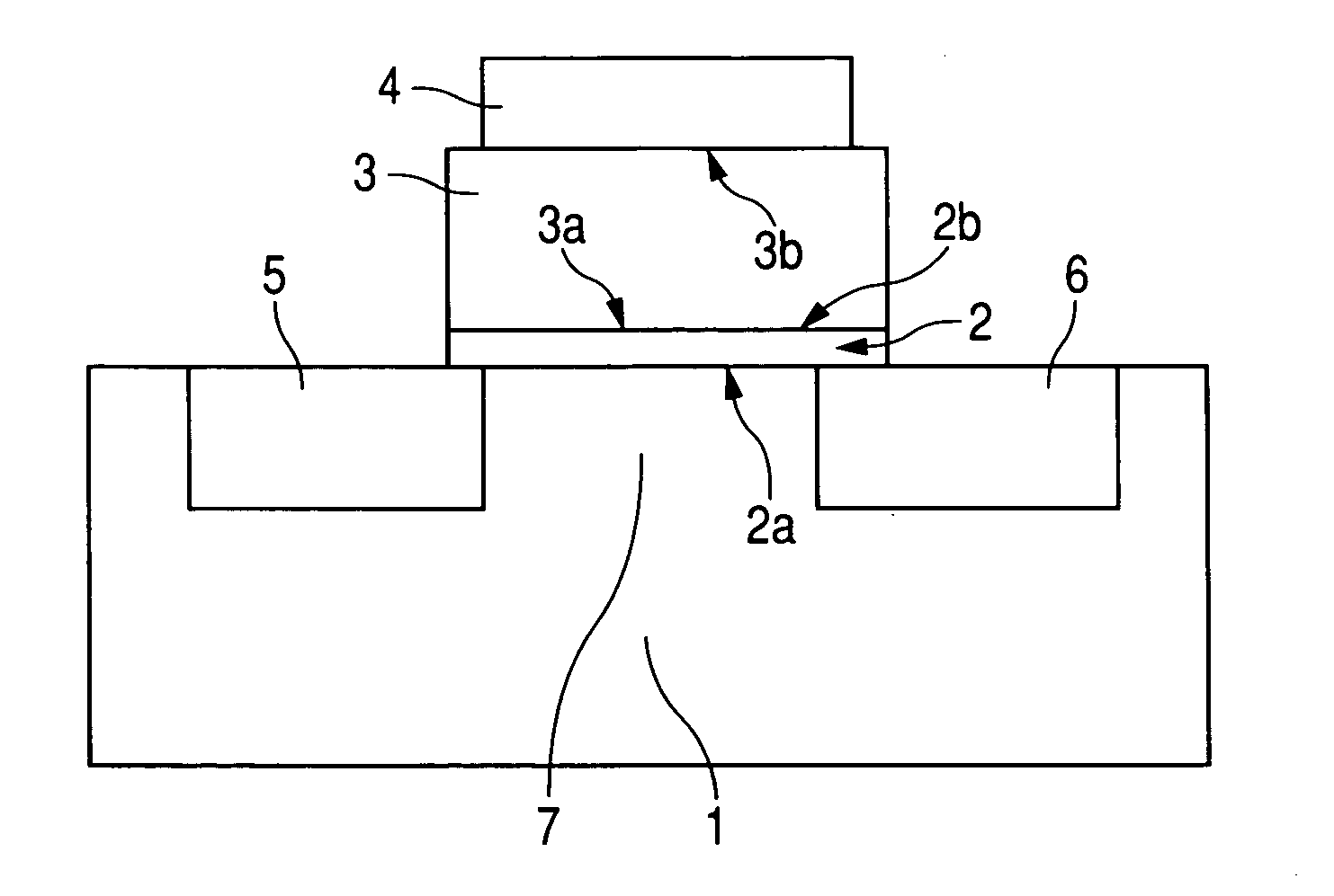
[0058] The materials used and the thicknesses thereof are as follows. [0059] Semiconductor substrate 1: Si [0060] Insulator buffer layer 2: Hf1−xAl2xO2+x+y; x=0.25; y=0; thickness of 10 nm [0061] Ferroelectric film 3: SrBi2Ta2O9; thickness of 400 nm [0062] Gate electrode 4: Pt; thickness of 200 nm; gate length (length of distance from source region to drain region) of 10 μm [0063] Conductivity type of source region 5 and drain region 6: n-type [0064] Conductivity type of region 7: p-type

[0065] Hf1−xAl2xO2+x+y (x=0.25; y=0) as an insulator buffer layer 2 was formed by pulsed-laser deposition. The laser used was a KrF excimer laser. The laser energy was 250 mJ per pulse, the pulse repetition frequency was 2 Hz, and the deposition time was 270 seconds. The temperature of the substrate was 200° C. The introduction gas was a nitrogen / oxygen mixed gas, in which the molar ratio N:O was 1:10−6. The pressure of this introduction gas in the deposition chamber was 0.1 Torr (13.33 Pa). SrBi2Ta...

example 2

[0067] The materials used and the thicknesses thereof are as follows. [0068] Semiconductor substrate 1: Si [0069] Insulator buffer layer 2: HfO2+u; u=0; thickness of 10 nm [0070] Ferroelectric film 3: SrBi2Ta2O9; thickness of 400 nm [0071] Gate electrode 4: Pt; thickness of 200 nm; gate length (length of distance from source region to drain region) of 10 μm [0072] Conductivity type of source region 5 and drain region 6: n-type [0073] Conductivity type of region 7: p-type

[0074] HfO2+u (u=0) as an insulator buffer layer 2 was formed by pulsed-laser deposition. The laser used was a KrF excimer laser. The laser energy was 250 mJ per pulse, the pulse repetition frequency was 2 Hz, and the deposition time was 270 seconds. The temperature of the substrate was 200° C. The introduction gas was a nitrogen / oxygen mixed gas, in which the molar ratio N:O was 1:10−6. The pressure of this introduction gas in the deposition chamber was 0.1 Torr (13.33 Pa). SrBi2Ta2O9 corresponding to a ferroelectr...

examples 3 to 7 and reference example

[0083] Transistors of Examples 3 to 7 were produced under completely the same conditions as in Example 1 and Example 2, except for the composition x in the insulator buffer layer. The values of x were: x=0.05 in Example 3, x=0.12 in Example 4, x=0.48 in Example 5, x=0.68 in Example 6, and x=0.85 in Example 7. Furthermore, a transistor employing a material in which x=1, i.e., Al2O3, as an insulator buffer layer was also produced as Reference Example. The gate voltage was swept and the drain current was measured to determine the memory window width of the MFIS transistor. The sweep gate voltage was conducted under the same conditions of ±6 V. The results thereof are shown in FIG. 11 together with the results in Example 1 and Example 2. The numerals in FIG. 11 correspond to the Example numbers. R in FIG. 11 indicates Reference Example. When x is equal to 0 or is in the range of from above 0 to below 0.7, memory window widths of 1 V or larger were obtained. A gate voltage VG of 7 V was ...


PUM

PropertyMeasurementUnit
molar ratioaaaaaaaaaa
thicknessaaaaaaaaaa
thicknessaaaaaaaaaa

Abstract

The MFIS transistors heretofore have a problem that after data writing, the data disappear in terms of memory transistor operation in about one day at most. This is mainly because the buffer layer and the ferroelectric have a high leakage current and, hence, charge is accumulated around the interface between the ferroelectric and the buffer layer so as to shield the electric polarization memorized by the ferroelectric, making it impossible for the electric polarization of the ferroelectric to control electrical conduction between the source and the drain in the transistor. In the present invention, by constituting an insulator buffer layer 2 of HfO2+u or Hf1−xAl2xO2+x+y, the leakage current flowing through each of the insulator buffer layer 2 and a ferroelectric 3 can be reduced and a memory transistor having a truly sufficient long data holding time is realized.

Description

TECHNICAL FIELD [0001] The present invention relates to semiconductor-ferroelectric storage devices and processes for producing the same. More particularly, the present invention relates to semiconductor-ferroelectric storage devices employing as a memory cell a transistor comprising a ferroelectric film in a gate insulation film, and processes for producing the devices. BACKGROUND ART [0002] Transistors employing a ferroelectric as a gate insulation film are expected to be next-generation highly integrated memories because data storage, data readout, and writing are conducted in the individual transistors. In this kind of transistor, electrical conduction in the transistor is controlled according to the direction of electric polarization of the ferroelectric. Virtually, structures comprising an insulator buffer layer inserted between a semiconductor and a ferroelectric so as not to impair the features of both of the semiconductor and the ferroelectric have been investigated (see, f...

Claims


Application Information

Patent Timeline
Patent Type & Authority Applications(United States)
IPC IPC(8): H01L29/78H01L21/336C23C14/08C23C16/40H01L21/28H01L21/316H01L21/8246H01L27/105H01L29/51
CPCC23C16/40H01L21/28291H01L21/31604H01L29/78391H01L21/31683H01L29/516H01L21/31616H01L29/40111H01L21/02178H01L21/02194H01L21/02181H01L29/6684
Inventor SAKAI, SHIGEKI
Owner NAT INST OF ADVANCED IND SCI & TECH
Why Eureka
Try Eureka