Ultraviolet assisted porogen removal and/or curing processes for forming porous low k dielectrics

a low-k dielectric and curing process technology, applied basic electric elements, electrical equipment, etc., can solve the problems of difficult removing of porogen, insufficient scaling down of devices, and inability to integrate porous low-k materials in the manufacture of semiconductor devices, etc., to achieve the effect of effectively removing porogen materials

Inactive Publication Date: 2006-02-02
AXCELIS TECHNOLOGIES
View PDF6 Cites 140 Cited by
  • Summary
  • Abstract
  • Description
  • Claims
  • Application Information

AI Technical Summary

Benefits of technology

[0012] In yet another embodiment, the process for forming an electrical interconnect structure comprises depositing a non-porous dielectric material comprising a matrix and a porogen material onto a substrate; exposing the non-porous dielectric film to a first ultraviolet radiation pattern, wherein the first ultraviolet radiation pattern is effective to increase the crosslinking density of the non-porous dielectric film, and wherein a concentration of the

Problems solved by technology

Considerable attention has been focused on electrically isolating the conductors from each other using new insulators having low dielectric constants because although silica (SiO2), which has traditionally been used in such devices because of its relatively low dielectric constant of about 4 and met the requirements of earlier (i.e., larger) applications, it will not be adequate as devices scale down.
However, the integration of porous low-k materials in the manufacture of the semiconductor device, in general, has proven difficult.
One major issue with porogen-based low k dielectrics lies in the difficulty with removing the porogen without leaving residual porogen fragments and without adversely affecting the rest of the dielectric material or other components in the semiconductor device.
These thermal processes may exceed the allowable thermal budgets for device manufacture.
Moreover, the introduction of pores into the dielectric material in this manner can reduce the overall mechanical strength, cohesive strength and fracture toughness of the porous dielectric material.
In addition to affecting the thermal and mechanical properties, the so-cured porous dielectric materials may have relatively poor moisture resistance and wet etching resistance, an area of concern where improvement is generally d

Method used


Image

  • Ultraviolet assisted porogen removal and/or curing processes for forming porous low k dielectrics
  • Ultraviolet assisted porogen removal and/or curing processes for forming porous low k dielectrics
  • Ultraviolet assisted porogen removal and/or curing processes for forming porous low k dielectrics

Examples


example 1

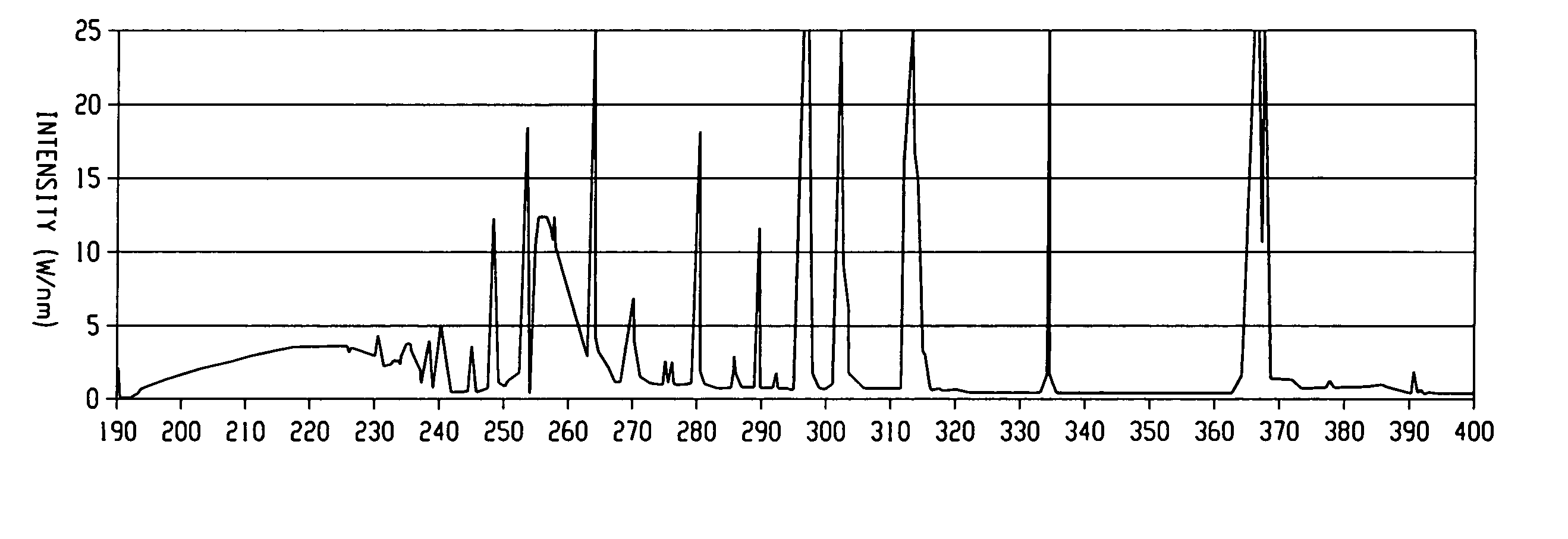
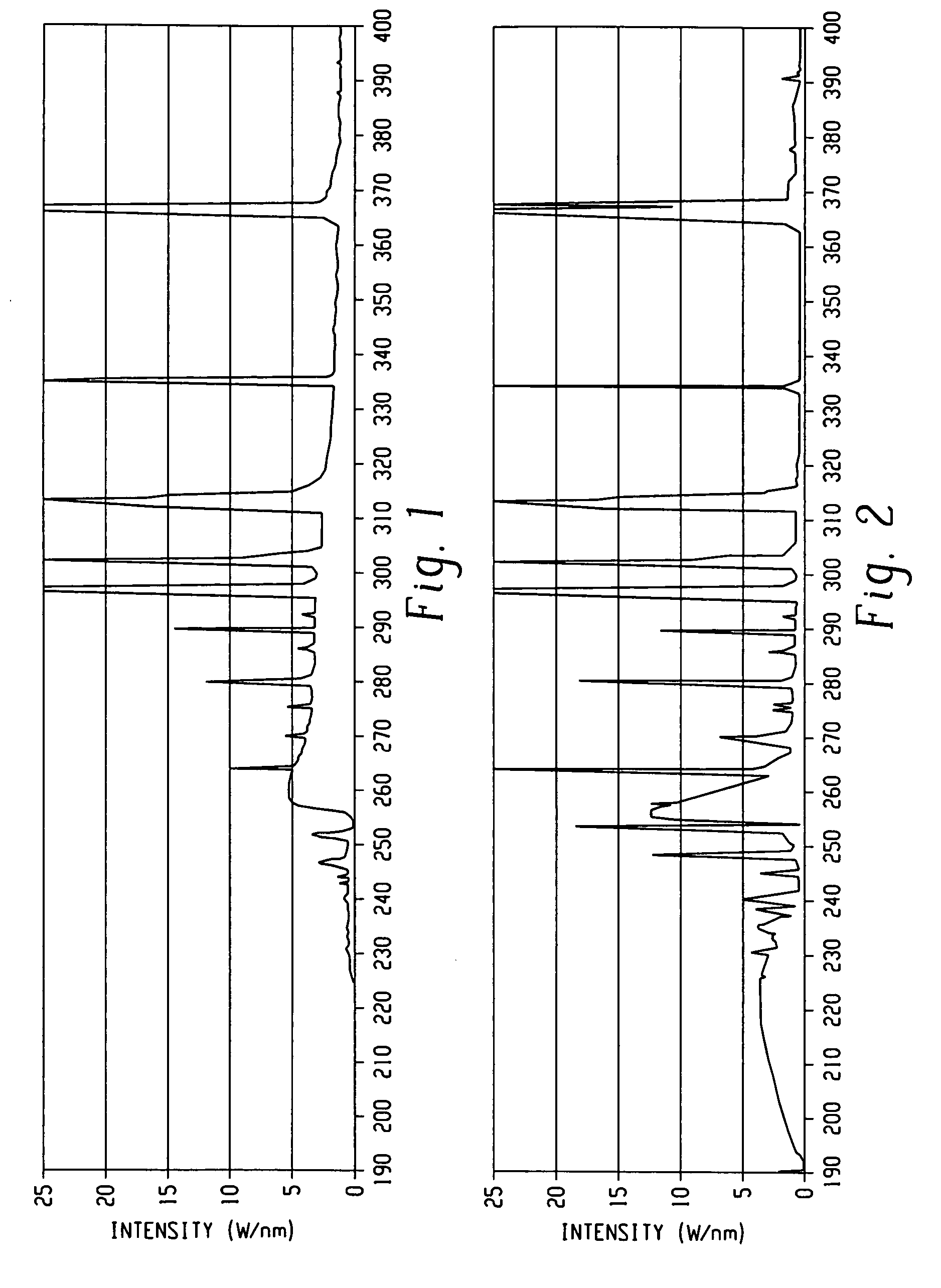
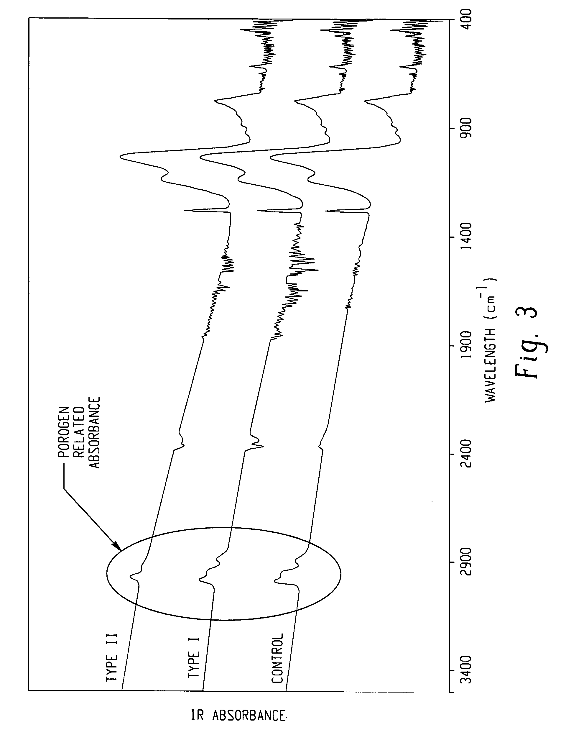
[0056] In this example, silicon substrates that contained a proprietary CVD deposited SiCOH porogen containing films were provided by a manufacturer. The films were exposed to different ultraviolet radiation patterns at 350° C. in a RapidCure Exposure tool available from Axcelis Technologies, Inc. and subjected to FTIR analysis. The ultraviolet radiation pattern was produced with Type I or Type II microwave electrodeless bulbs in an inert atmosphere. A control that did not include exposure to UV radiation was included in the analysis. As shown in FIG. 3, the porogen related absorbance at about 3,000 cm−1 clearly illustrates a dependence on wavelength exposure. Exposure to ultraviolet radiation having no substantial radiation at wavelengths less than 240 nm (Type I bulb, spectra shown in FIG. 1) did not exhibit any detectable amounts of porogen removal since the absorbance spectra for exposure to wavelengths greater than 240 nm was clearly similar to the control. In contrast, exposur...

example 2

[0057] In this example, silicon substrates that contained a proprietary CVD deposited SiCOH porogen containing film were provided by a manufacturer. The substrates were processed in accordance with Example 1 using a Type I microwave electrodeless bulb. FIG. 4 illustrates the spectra before and after UV exposure. As is evidenced by the peak absorption at about 950 cm−1, exposure to UV radiation caused a broadening in absorption intensity related to Si—O crosslinking, indicating an increase in Si—O crosslinking (primarily caused by a decrease in Si—OH functionality, the peak associated with S1—CH3 absorbance at about 1300 cm−1 did not change before or after exposure). Analysis of the intensity pattern related to porogen absorption at about 3000 cm−1 showed that the porogen remains in the low k dielectric film after exposure to the ultraviolet radiation.


PUM


Abstract

Processes for forming porous low k dielectric materials from low k dielectric films containing a porogen material include exposing the low k dielectric film to ultraviolet radiation. In one embodiment, the film is exposed to broadband ultraviolet radiation of less than 240 nm for a period of time and intensity effective to remove the porogen material. In other embodiments, the low k dielectric film is exposed to a first ultraviolet radiation pattern effective to increase a crosslinking density of the film matrix while maintaining a concentration of the porogen material substantially the same before and after exposure to the first ultraviolet radiation pattern. The low k dielectric film can be then be processed to form a metal interconnect structure therein and subsequently exposed to a second ultraviolet radiation pattern effective to remove the porogen material from the low k dielectrics film and form a porous low k dielectric film.

Description

CROSS REFERENCE TO RELATED APPLICATIONS [0001] The present application relates to and claims priority to U.S. Provisional Application No. 60 / 577,726 filed on Jun. 7, 2004, incorporated herein by reference in its entirety.BACKGROUND [0002] The present disclosure generally relates to the manufacture of semiconductor devices, and more particularly, to ultraviolet assisted porogen removal and / or curing processes for forming porous low k dielectric materials employed in semiconductor devices. [0003] As semiconductor and other microelectronic devices progressively decrease in size, the demands placed on device components continue to increase. For example, the prevention of capacitive crosstalk between interconnect lines becomes significantly more important with smaller devices. Capacitive crosstalk is generally a function of both the distance between conductors and the dielectric constant (k) of the material (i.e., the insulator) placed in between the conductors. Considerable attention ha...

Claims


Application Information

Patent Timeline
IPC IPC(8): H01L21/31H01L21/26
CPCH01L21/02126H01L21/02203H01L21/02271H01L2221/1047H01L21/31695H01L21/7682H01L21/76825H01L21/02348
Inventor WALDFRIED, CARLOHAN, QINGYUANESCORCIA, ORLANDOBERRY, IVAN III
Owner AXCELIS TECHNOLOGIES
Why Eureka
Try Eureka