Method and system for source switching and in-situ plasma bonding

Active Publication Date: 2006-02-09
SILICON GENERAL CORPORATION
View PDF16 Cites 11 Cited by
  • Summary
  • Abstract
  • Description
  • Claims
  • Application Information

AI Technical Summary

Benefits of technology

[0011] In yet another specific embodiment, the present invention provides a technique for processing substrates using a novel cluster tool apparatus. The apparatus includes, among other elements, a transfer chamber comprising a robot therein. A plasma chamber is coupled to the transfer chamber, and a third chamber is coupled to the transfer chamber. The third chamber can be selected from at least a CVD chamber, an etch chamber, a PVD chamber, a thermal annealing chamber, a bonding chamber, a CCP (controlled cleavage process) chamber, a CMP (chemical mechanical polishing) chamber, a thermal treatment chamber, a plasma immersion ion implantation treatment chamber, an epitaxial growth chamber, and others. The present apparatus can process a plurality of substrates without breaking vacuum, which enhances process quality and device yields, among other factors. Alternatively, the substrates are processed at atmospheric conditions.
[0012] In another specific embodiment, the present invention provides an apparatus having a memory for processing substrates using a novel cluster tool apparatus. The memory has a computer program in the form of software, which can be in the form of computer codes or the like. The codes include one or more for operating a transfer chamber comprising a robot therein. The codes also include one or more for operating (e.g., turning on and off) a plasma treatment chamber that is coupled to the transfer chamber. A computer code also exists for operating a third chamber that is coupled to the transfer chamber. The third chamber can be selected from at least a CVD chamber, an etch chamber, a PVD chamber, a thermal annealing chamber, a bonding cham

Problems solved by technology

These techniques, however, are not free from limitations.
For example, conventional isolation techniques consume a considerable amount of valuable wafer surface area on the chip, and often generate a non-planar surface as an artifact of the isolation process.
Either or both of these considerations generally limit the degree of integration achievable in a given chip.
Additionally, trench isolation often requires a process of reactive ion etching, which is extremely time consuming and can be difficult to achieve accurately.
Bulk silicon wafers, which are greater than 200 millimeters, are not free from defects and can reduce overal

Method used


Image

  • Method and system for source switching and in-situ plasma bonding
  • Method and system for source switching and in-situ plasma bonding
  • Method and system for source switching and in-situ plasma bonding

Examples


Example

[0022] According to the present invention, techniques for the manufacture of substrates are provided. More particularly, the invention provides a technique including a method and device for treating a first substrate to a second substrate for the manufacture of semiconductor integrated circuits, for example. But it will be recognized that the invention has a wider range of applicability; it can also be applied to other substrates for multi-layered integrated circuit devices, three-dimensional packaging of integrated semiconductor devices, photonic devices, piezoelectronic devices, microelectromechanical systems (“MEMS”), sensors, actuators, solar cells, flat panel displays (e.g., LCD, AMLCD), biological and biomedical devices, and the like.

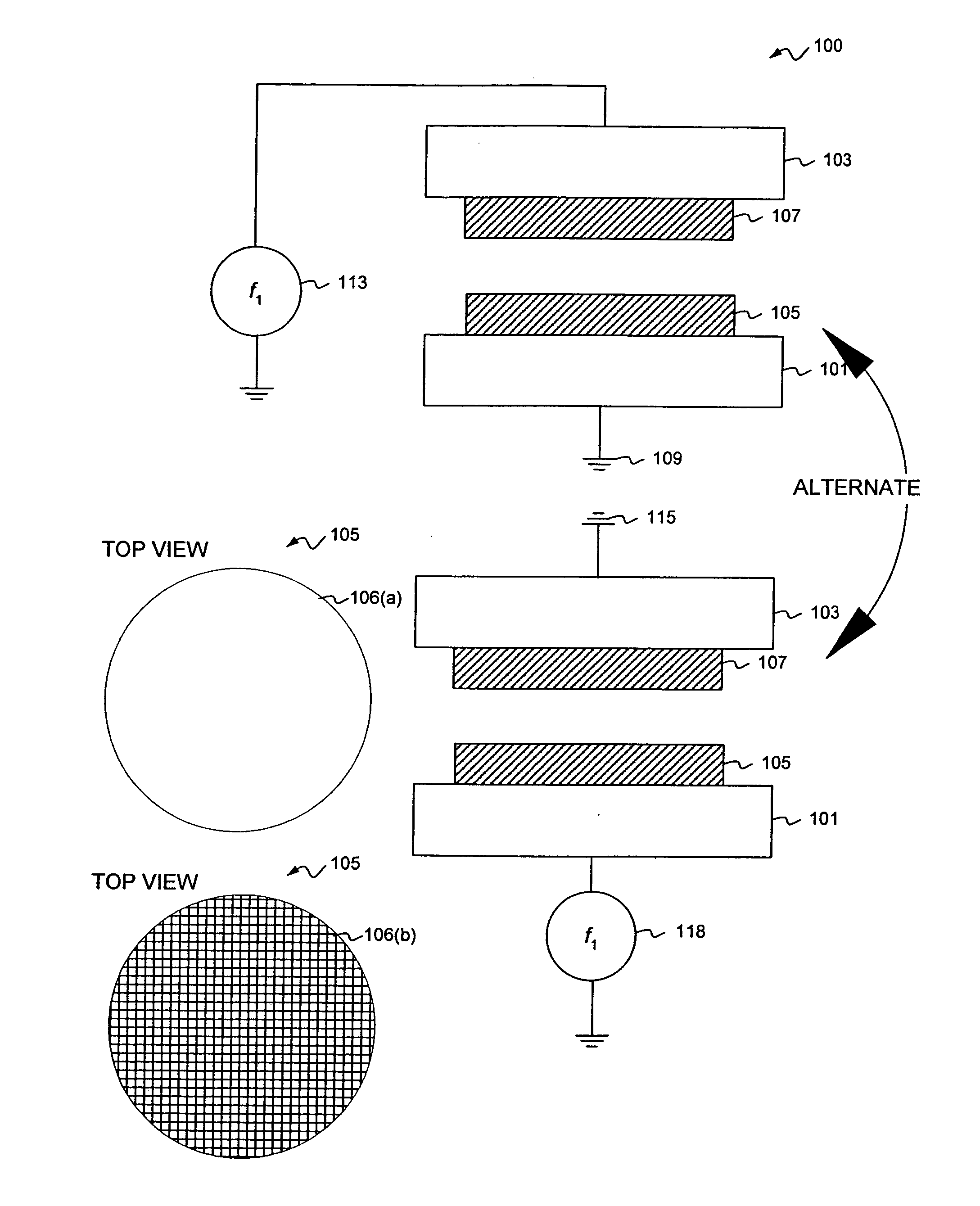
[0023]FIG. 1 is a simplified diagram of a treatment system according to an embodiment of the present invention. This diagram is merely an example, which should not unduly limit the scope of the claims herein. One of ordinary skill in the art woul...


PUM


Abstract

A system for in-situ plasma treatment. The system has a processing chamber, e.g., plasma chamber. The system has a first susceptor coupled within the chamber and a second susceptor facing the first susceptor and being within the chamber. The system has one or more power sources. Preferably, a first power source is characterized by a first frequency. The first power source is coupled to the first susceptor and the second susceptor. A second power source is characterized by a second frequency. The second power source is coupled to the first susceptor and the second susceptor. A switching device is coupled to the first power source and is coupled the second power source. The switching device is configured to selectively apply the first frequency to the first susceptor while the second frequency is applied to the second susceptor and is alternatively configured to selectively apply the first frequency to the second susceptor while the second frequency is applied to the first susceptor.

Description

BACKGROUND OF THE INVENTION [0001] The present invention relates to the manufacture of substrates. More particularly, the invention provides a technique including a method and device for treating a first substrate to a second substrate for the manufacture of semiconductor integrated circuits, for example. But it will be recognized that the invention has a wider range of applicability; it can also be applied to other substrates for multi-layered integrated circuit devices, three-dimensional packaging of integrated semiconductor devices, photonic devices, piezoelectronic devices, microelectromechanical systems (“MEMS”), sensors, actuators, solar cells, flat panel displays (e.g., LCD, AMLCD), biological and biomedical devices, and the like. [0002] Integrated circuits are fabricated on chips of semiconductor material. These integrated circuits often contain thousands, or even millions, of transistors and other devices. In particular, it is desirable to put as many transistors as possibl...

Claims


Application Information

Patent Timeline
IPC IPC(8): H01L21/26
CPCH01J37/32082H01J37/32706H01J37/32165
Inventor HENLEY, FRANCOIS J.
Owner SILICON GENERAL CORPORATION
Why Eureka
Try Eureka