Near infrared chemical imaging microscope

a chemical imaging and near infrared technology, applied in the direction of optical radiation measurement, instruments, spectrometry/spectrophotometry/monochromators, etc., can solve the problems of defective devices often left undiagnosed, difficult device fabrication and device processing defects, and difficult manufacturing of compound semiconductors

Inactive Publication Date: 2006-02-16
CHEMIMAGE TECH
View PDF1 Cites 22 Cited by
  • Summary
  • Abstract
  • Description
  • Claims
  • Application Information

AI Technical Summary

Benefits of technology

[0013] To address the need for a device that can provide video imaging, NIR spectroscopy and high resolution (spatial and spectral) NIR chemical imaging in two and three spatial dimensions, a novel NIR chemical imaging microscope has been developed that is NIR chemical imaging capable.
[0014] The microscope design uses NIR optimized liquid crystal (LC) imaging spectrometer technology for wavelength selection. The NIR optimized refractive microscope is used in conjunction with infinity-corrected objectives to form the NIR image on the detector with or without the use of a tube lens. An integrated parfocal analog color CCD detector provides real-time sample positioning and focusing. The color image and the NIR image are fused in software. In one configuration, the NIR microscope may be used as a volumetric imaging instrument through the means of moving the sample through focus, collecting images at varying focal depths and reconstructing a volumetric image of the sample in software, or through the means of keeping the sample fixed and changing the wavelength dependent depth of penetration in conjunction with a refractive tube lens with a well characterized chromatic effect. The output of the microscope can be coupled to a NIR spectrometer either via direct optical coupling or via a fiber optic. A Chemical Imaging Addition Method seeds the sample with a material of known composition, structure and / or concentration and then generates the NIR image suitable for qualitative and quantitative analysis. The microscope generates NIR chemical image data that is analyzed and visualized using chemical image analysis software in a systematic and comprehensive manner. While this invention has been demonstrated on a microscope optic platform, the novel concepts are also applicable to other image gathering platforms, namely fiberscopes, macrolens systems and telescopes.

Problems solved by technology

Compound semiconductors are challenging to fabricate.
Device fabrication and device processing defects can be difficult and time consuming to measure during manufacturing.
Unfortunately, defective devices are often left undiagnosed until latter stages in the manufacturing process because of the inadequacy of the metrology tools being used.
This results in low production yields and high costs which can be an impediment to growth in the semiconductor device market potential.
These devices are often decorated with microscopic and macroscopic defects limiting the yield of large-size, high-quality materials.
It has been demonstrated that the presence of tellurium inclusions can impair the electronic properties of CdZnTe materials—consequently degrading the end-product device performance.
The current procedure used by low volume semiconductor manufacturers for characterizing tellurium inclusions in CdZnTe is labor intensive, susceptible to human error and provides little information on inclusions in the 1-5 μm size scale.
This analysis is relatively time consuming, often taking several minutes to characterize a region of interest from a large wafer.
One of the biggest problems with the raw images collected is the gradually varying background across each image frame.
Defects such as tellurium inclusions affect the electrical properties in CdZnTe semiconductor materials, degrading end-product device performance.

Method used


Image

  • Near infrared chemical imaging microscope
  • Near infrared chemical imaging microscope
  • Near infrared chemical imaging microscope

Examples


example

Overview

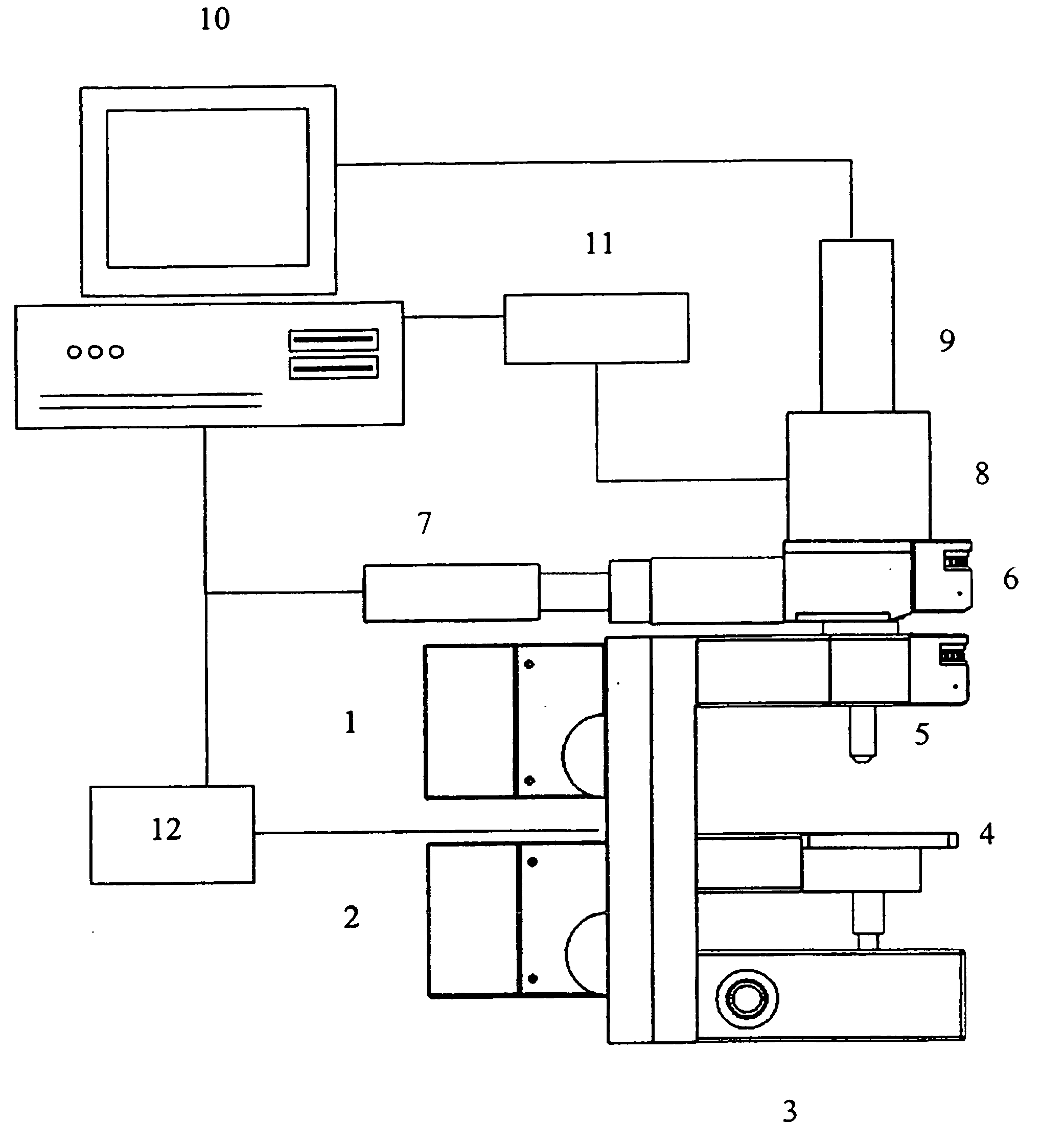
[0057] As the demand for high quality, low cost X-ray, γ-ray and imaging detector devices increases, there is a need to improve the quality and production yield of semiconductor materials used in these devices. One effective strategy for improving semiconductor device yield is through the use of better device characterization tools that can rapidly and nondestructively identify defects at early stages in the fabrication process. Early screening helps to elucidate the underlying causes of defects and to reduce downstream costs associated with processing defect laden materials that are ultimately scrapped. The present invention can be used to characterize tellurium inclusion defects in cadmium zinc telluride (CdZnTe) semiconductor materials based on near infrared imaging. With this approach, large area wafers can be inspected rapidly and non-destructively in two and three spatial dimensions by collecting NIR image frames at multiple regions of interest throughout the wafer u...


PUM

PropertyMeasurementUnit
wavelengthsaaaaaaaaaa
sizeaaaaaaaaaa
sizeaaaaaaaaaa

Abstract

A chemical imaging system is provided which uses a near infrared radiation microscope. The system includes an illumination source which illuminates an area of a sample using light in the near infrared radiation wavelength and light in the visible wavelength. A multitude of spatially resolved spectra of transmitted, reflected, emitted or scattered near infrared wavelength radiation light from the illuminated area of the sample is collected and a collimated beam is produced therefrom. A near infrared imaging spectrometer is provided for selecting a near infrared radiation image of the collimated beam. The filtered images are collected by a detector for further processing. The visible wavelength light from the illuminated area of the sample is simultaneously detected providing for the simultaneous visible and near infrared chemical imaging analysis of the sample. Two efficient means for performing three dimensional near infrared chemical imaging microscopy are provided.

Description

[0001] This application claims the benefit of U.S. Provisional Application No. 60 / 239,969, entitled “Near Infrared Chemical Imaging Microscope” filed Oct. 13, 2000. [0002] This work is supported by the National Institute of Standards and Technology (NIST) under the Advanced Technology Program (ATP) award (Contract Number 70NANB8H4021)FIELD OF INVENTION [0003] The present invention is related to near-infrared (NIR) microscopes for spectroscopic and image analysis, and, in particular, to microscopes useful for both NIR spectroscopy, NIR chemical imaging and NIR volumetric chemical imaging. BACKGROUND OF THE INVENTION [0004] NIR spectroscopy is a mature, non-contact, non-destructive analytical characterization tool that has been widely applied to a broad range of materials. The NIR region of the electromagnetic spectrum encompasses radiation with wavelengths of 0.78 to 2.5 μm (12,800 to 4,000 cm−1). NIR spectra result from the overtone and combination bands of fundamental mid-infrared ...

Claims


Application Information

Patent Timeline
Patent Type & Authority Applications(United States)
IPC IPC(8): G01N21/35G01J3/28G02B21/06
CPCG01J3/2823G02B21/06G02B21/0016G01N21/359
Inventor TREADO, PATRICK J.NELSON, MATTHEWKEITZER, SCOTT
Owner CHEMIMAGE TECH
Why Eureka
Try Eureka