The resulting undesirable presence of
copper causes
dielectric layers to become conductive and electronic devices to fail.
Carbon incorporation is often detrimental to the completion of wet chemical processes since the deposited film tends to be hydrophobic, reducing or preventing fluids from
wetting and depositing a film having desirable properties.
Another problem with the use of copper and its alloys is that copper readily oxidizes when exposed to air and is also vulnerable to
chemical corrosion and deterioration due to subsequent
processing steps.
Copper interconnects are adversely affected by oxidation and other forms of deterioration and seed layers suffer from widely different levels of oxidation when
queue times vary between lots.
One problem with previous capping layer methods is inadequate pre-treatment of the substrate prior to
electroless deposition of the capping layer and inadequate post-treatment of the capping layer, which may cause
contamination problems and / or selectivity problems.
The presence of this type of
contamination can seriously affect subsequent electroless deposition as well as other processing steps.
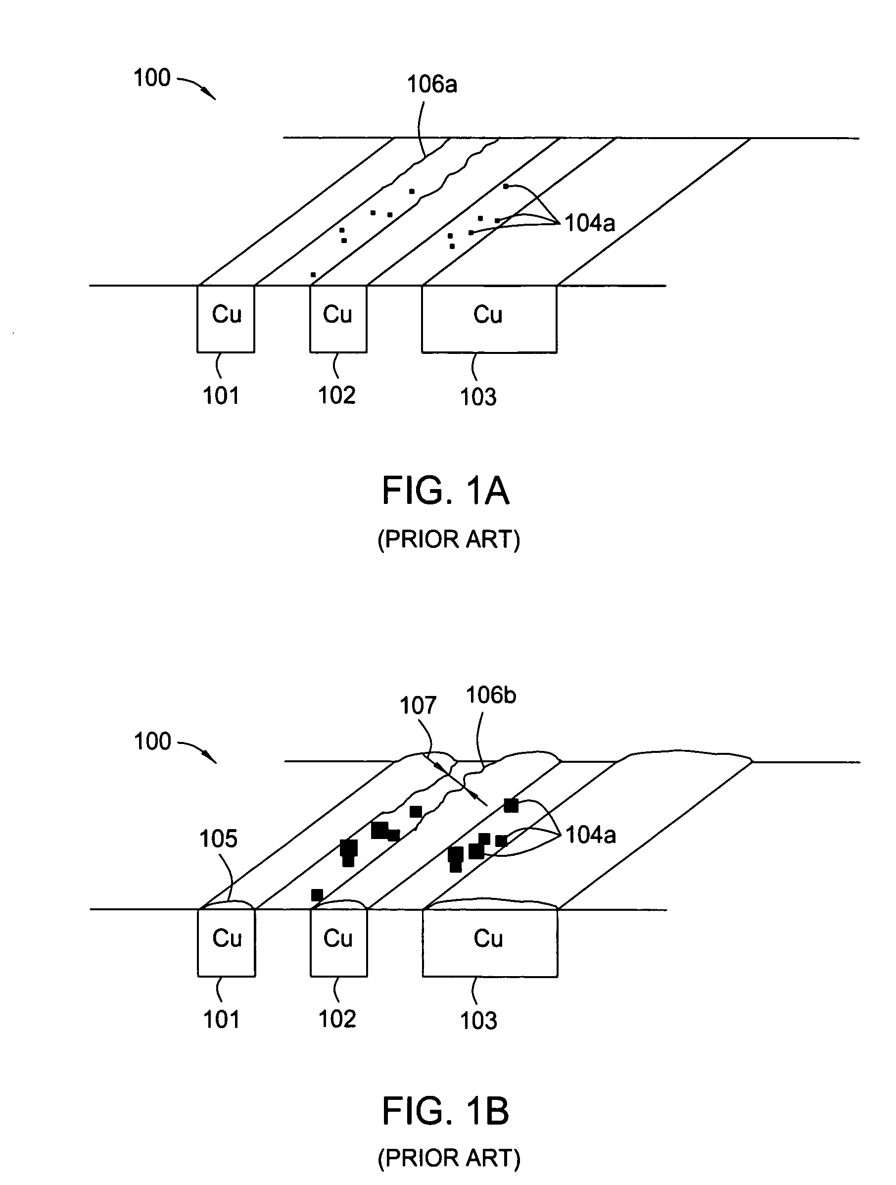
Another problem with using capping layers to protect interconnects is the potential creation of shorts between closely spaced interconnects. FIG. 1A illustrates a substrate structure 100 with parallel interconnects 101, 102 and 103.
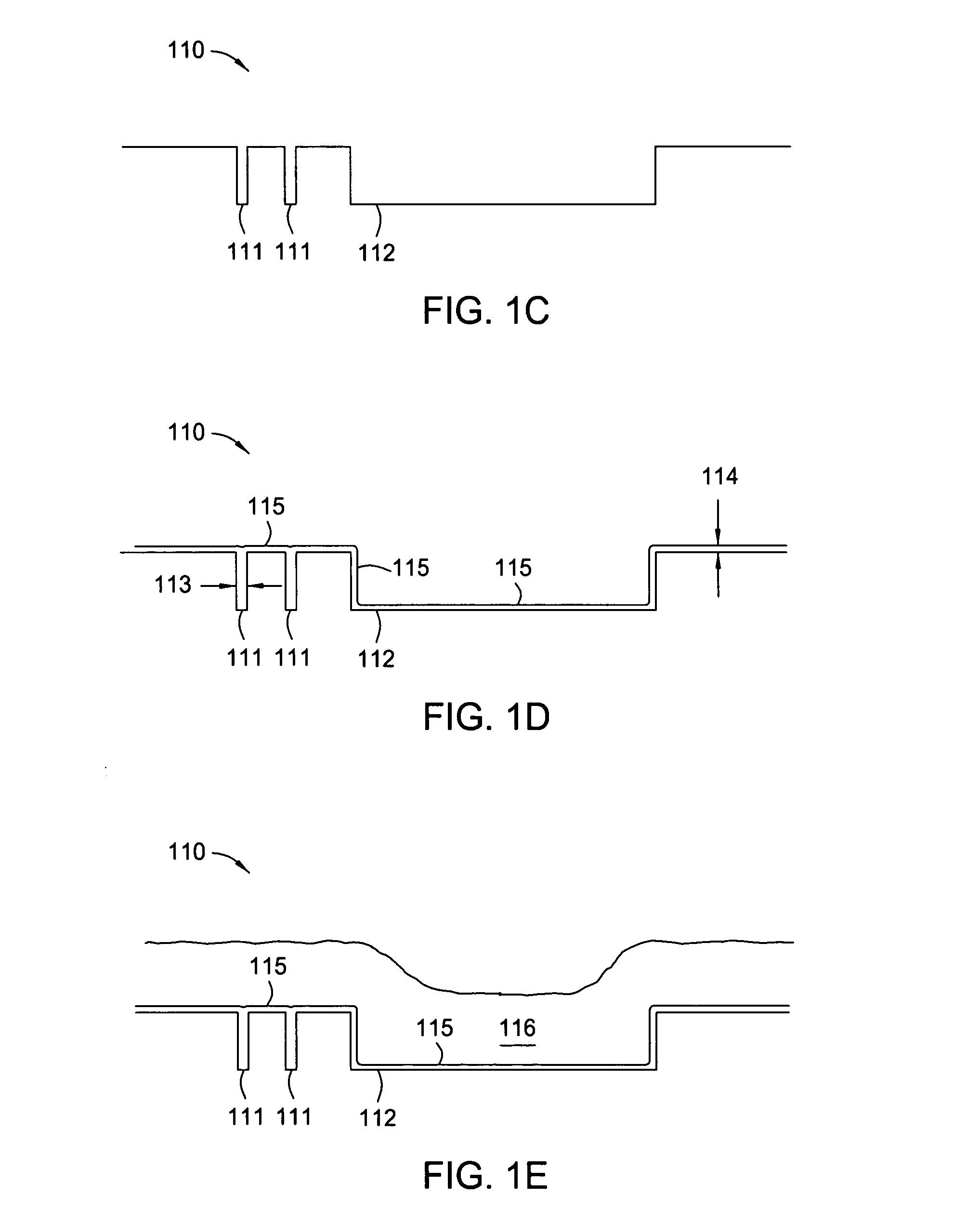
Another problem facing manufacturers of ultra-large scale integrated circuits is the filling of very high and very low
aspect ratio features on the same device at the same time. FIG. 1C is a
schematic side view of a substrate structure 110 with sub-micron high
aspect ratio (i.e., >10:1) features, such as high
aspect ratio features 111, and a low aspect ratio feature 112, both requiring copper fill.
Electroless deposition of films that can fill such large substrate features can require prohibitively long deposition times, e.g. one or more orders of magnitude longer than the time required to fill high aspect ratio features 111.
Application of a second plating method to fill low aspect ratio features such as 112 typically requires the added expense and complexity of processing substrates on an additional processing platform.
Another problem related to oxidation is the formation of a native
oxide on exposed
electrical contacts during the fabrication of electronic devices.
Native
oxide films are usually very thin, such as between 5 and 20 angstroms, but thick enough to cause difficulties in subsequent fabrication processes.
Such difficulties usually affect the electrical properties of
semiconductor devices formed on the substrate.
For example, a particular problem arises when native
silicon oxide films are formed on exposed contact surfaces (e.g., source or drain connection points), such as those shown in FIG. 1C.
Native oxides are electrically insulating and are undesirable at interfaces with device contacts or interconnecting electrical pathways because they cause high electrical
contact resistance.
This results in lower substrate yields and increased failure rates due to overheating at the
electrical contacts.
Sputter
etching performs poorly in features having aspect ratios smaller than about 4:1 and can damage delicate
silicon layers by physical bombardment.
Wet etch processes also perform poorly in high aspect ratio features and may contaminate the feature with undesirable
fluorine contamination.
Ultra-large scale integrated circuits may also suffer from high
contact resistance as devices on integrated circuits are further reduced in size.
Contamination may be present inside high aspect ratio features 111 from previous process steps because it is difficult to remove from such features.
Similarly, unwanted voids tend to form in high aspect ratio contacts when the contacts are filled with
tungsten using conventional CVD methods.
Because barrier layers generally posses worse-than-optimal electrical resistance,
contact resistance increases exponentially with decreasing size when conventional barrier layers are used.
Yet another problem that occurs during the manufacture of ultra-large scale integrated circuits is the depletion of
silicon at the source / drain contact interface through silicidation, i.e.,
diffusion into the contact interface by the conductive material filling the contact feature and the subsequent formation of a
silicide by the conductive fill material.
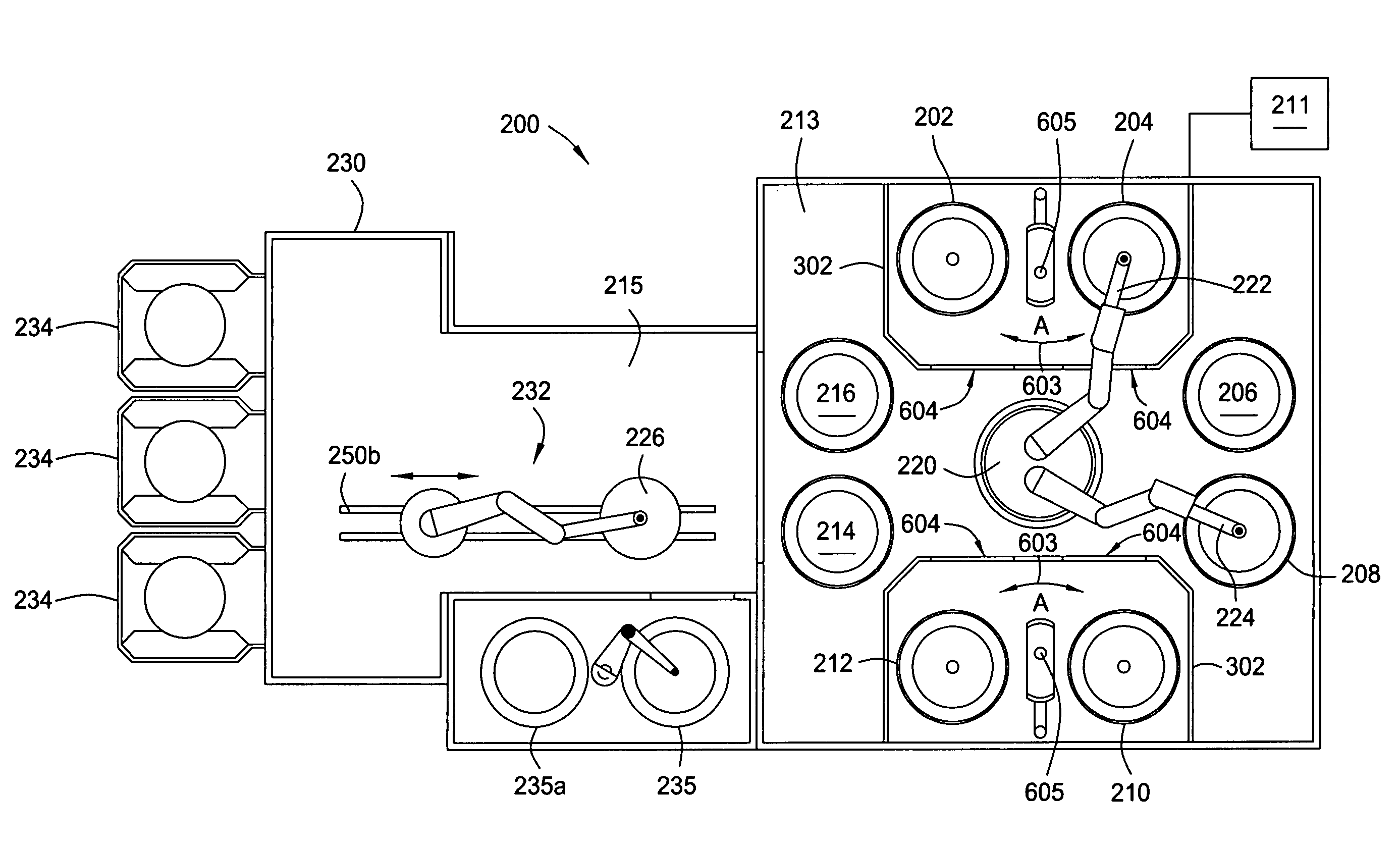
Further, a functional and efficient integrated platform for electroless deposition processes capable of depositing uniform layers with minimal defects has not been developed.

