White light-emitting device and method for preparing the same

a light-emitting device and white light-emitting technology, which is applied in the direction of discharge tube luminescnet screens, energy-saving lighting, sustainable buildings, etc., can solve the problems of low luminescent and phosphor conversion efficiency, inefficient light-emitting sources, and commercial optoelectronic products

Inactive Publication Date: 2006-03-02
INST NUCLEAR ENERGY RES ROCAEC
View PDF3 Cites 3 Cited by
  • Summary
  • Abstract
  • Description
  • Claims
  • Application Information

AI Technical Summary

Problems solved by technology

Since there are differences such as the driving voltage, optical output, temperature characteristic and life span between the red, green and blue light-emitting diodes, many problems arise when this method is actually conducted.
This method needs only one light source and is easier for designing the driving circuits, but the luminescent and transforming efficiency from electricity to light of the phosphor is too low.
At room temperature, silicon (an element of IV group in the periodic table) is an inefficient light-emitting source because it is one of the indirect band-gap materials with very low radioactive recombination rate and internal quantum efficiency of only about 10−6 to 10−7, so that silicon has not been used as a light-emitting source.
However, there are still not any commercial optoelectronic products such as the LED so far in spite of preferable result in research and development of the silicon-based LED at present.
Due to the sponge-like structure, the porous silicon has some major defects in the application of the light-emitting device.
As to the mechanical property, it is inappropriate to integrate the porous silicon with the standard semiconductor fabrication process for the frangibility of the former.
In addition, the porous silicon is highly reactive in chemical properties and is likely to react with oxygen in the atmosphere, which results in the degradation of the photoelectric property.
The degradation of the photoelectric property causes more difficulty in controlling the variation of the photoelectric properties with time.

Method used


Image

  • White light-emitting device and method for preparing the same
  • White light-emitting device and method for preparing the same
  • White light-emitting device and method for preparing the same

Examples


Embodiment Construction

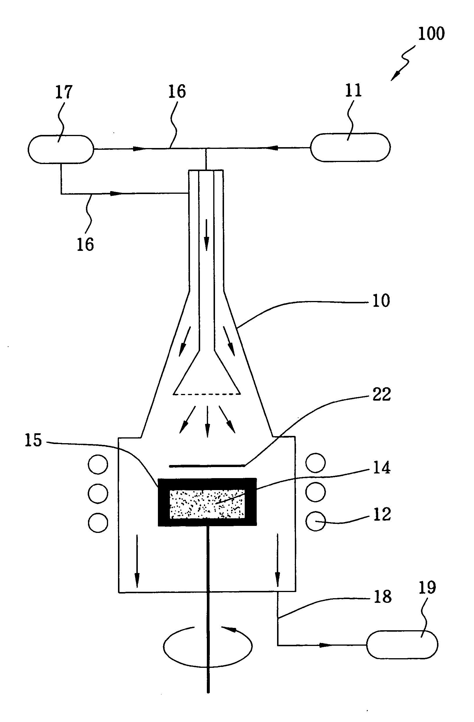
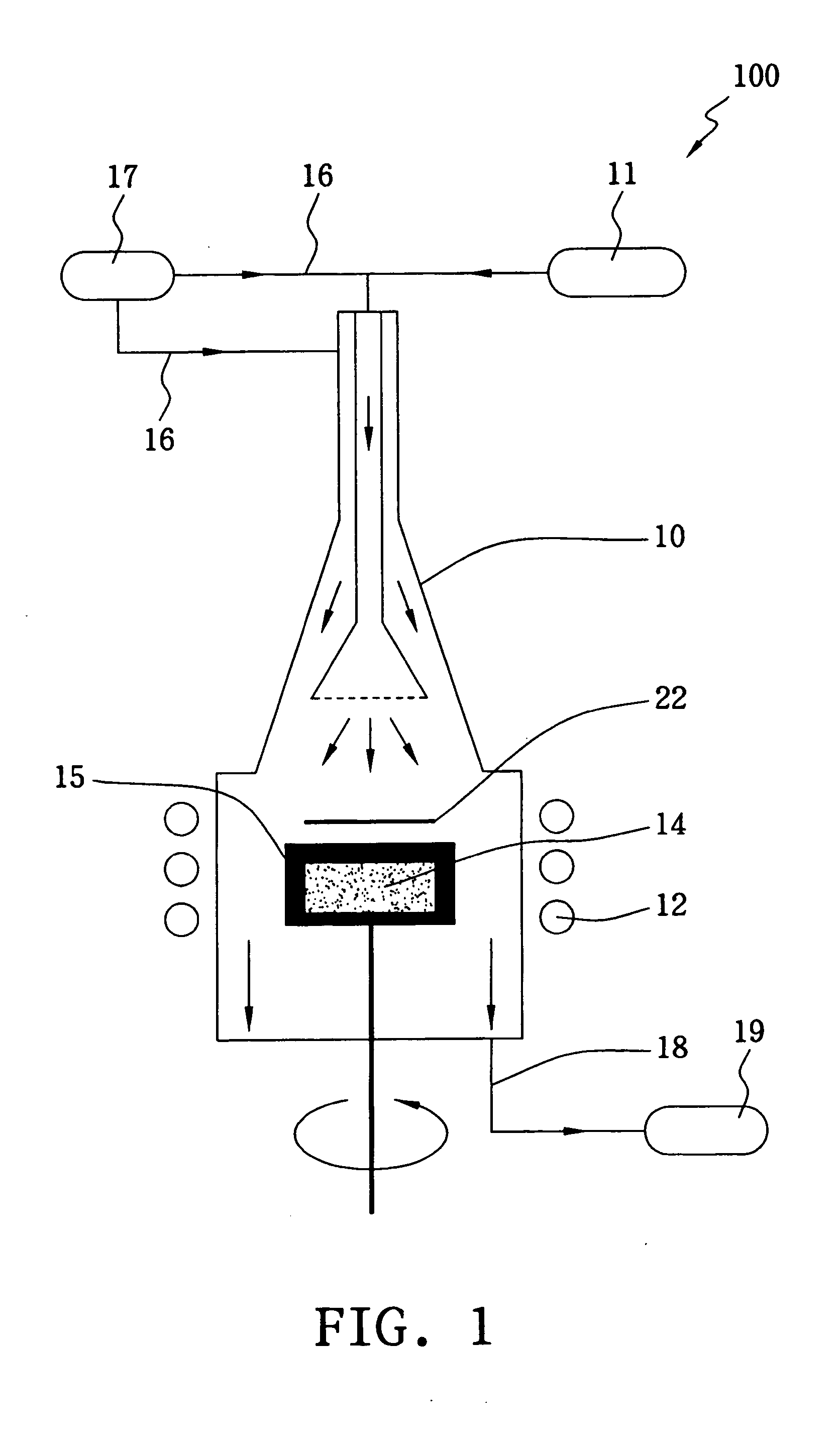
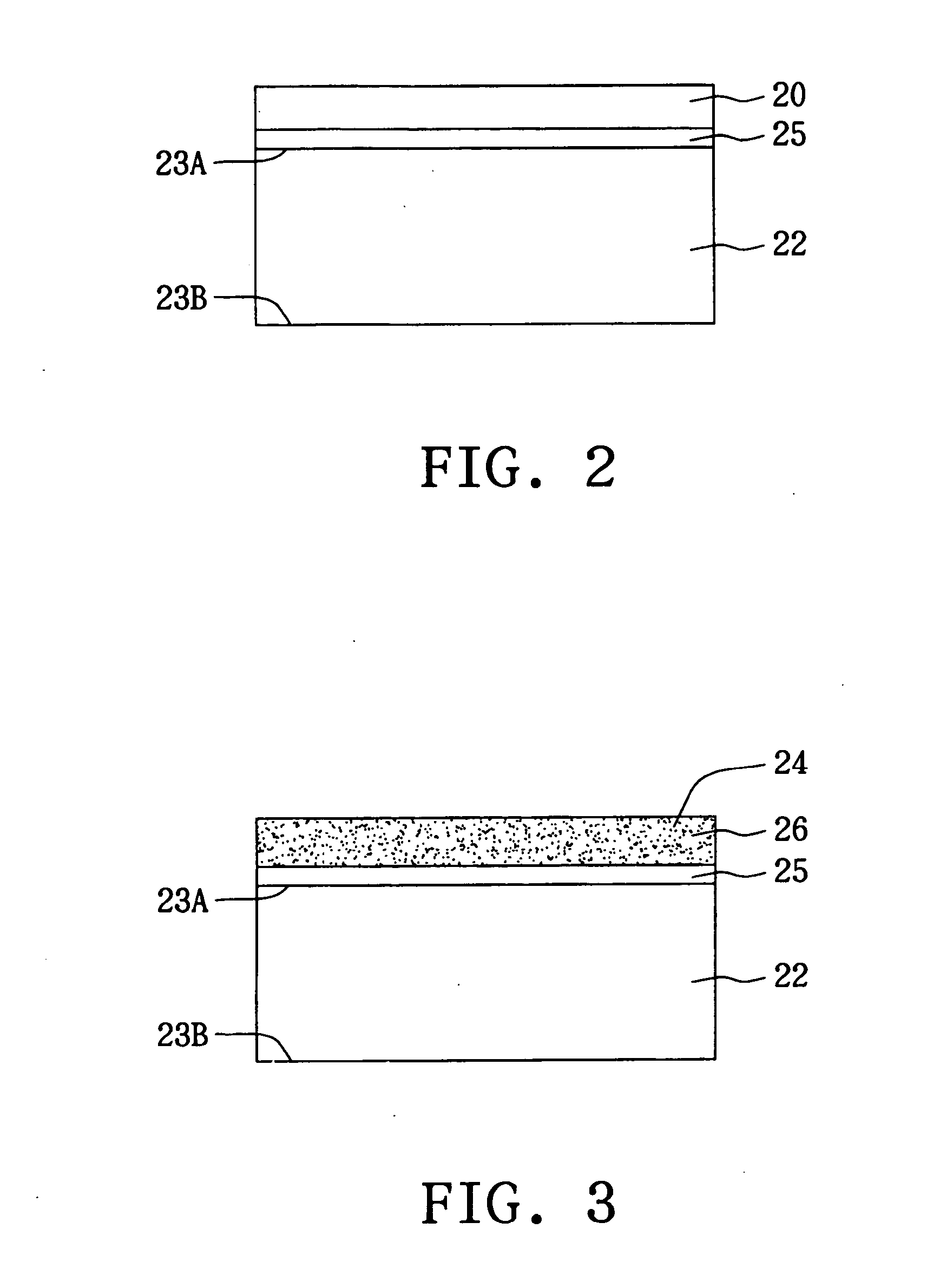
[0022] The quantum confinement effect broadens the band-gap of materials as the size of the material becomes smaller, and the nanocrystal has a distinct photoelectric property from the ordinary crystal with a larger size. Therefore, besides the well-known porous silicon, researchers also attempted to prepare the silicon-based light source by generating silicon nanocrystals (Si—NC) in a highly stable silicon dioxide layer. However, silicon nanocrystals (Si—NC) in the silicon dioxide layer can only emit red light or infra-red light. The present invention prepares silicon nanocrystals (Si—NC) in a trisilicon tetranitride layer to emit a white light with a wavelength between 400 and 700 nanometers.

[0023] One of methods for preparing the Si—NC, which is capable of emitting red light or infra-red light, first forms a sub-stoichiometric silica (SiOx) layer with excess of silicon atoms by chemical vapor deposition (CVD), wherein the numerical ratio (x) of oxygen atoms to silicon atoms is s...


PUM


Abstract

The present white light-emitting device includes a substrate with first window layer, a trisilicon tetranitride layer positioned on the first window layer, a plurality of silicon nanocrystals distributed in the trisilicon tetranitride layer, a second window layer, a transparent conductive layer and a first ohmic contact electrode positioned in sequence on the trisilicon tetranitride layer, and a second ohmic contact electrode positioned on the bottom surface of the substrate. The present method first forms a sub-stoichiometric silicon nitride (SiNx) layer on a substrate, wherein the numerical ratio (x) of nitrogen atoms to silicon atoms is smaller than 4 / 3. A thermal treating process is then performed to transform the sub-stoichiometric SiNx layer into a trisilicon tetranitride layer with a plurality of silicon nanocrystals distributed therein. The thickness of the trisilicon tetranitride layer is between 1 and 10,000 nanometers, and the diameter of the silicon nanocrystal is between 1 and 10 nanometers.

Description

RELATED U.S. APPLICATIONS [0001] Not applicable. STATEMENT REGARDING FEDERALLY SPONSORED RESEARCH OR DEVELOPMENT [0002] Not applicable. REFERENCE TO MICROFICHE APPENDIX [0003] Not applicable. FIELD OF THE INVENTION [0004] The present invention relates to a white light-emitting device and method for preparing the same, and more particularly, to a white light-emitting device with a silicon-containing active layer and method for preparing the same. BACKGROUND OF THE INVENTION [0005] There are two methods for generating white light using a light-emitting device. One of the two methods uses the mixing of the red, green and blue lights to generate the white light by turning on a red light-emitting diode, a green light-emitting diode and a blue light-emitting diode simultaneously. Since there are differences such as the driving voltage, optical output, temperature characteristic and life span between the red, green and blue light-emitting diodes, many problems arise when this method is act...

Claims


Application Information

Patent Timeline
Patent Type & Authority Applications(United States)
IPC IPC(8): H01J1/62H01J63/04
CPCB82Y20/00C09K11/02C09K11/0883Y02B20/181H01L33/34H05B33/14C09K11/59Y02B20/00
Inventor YANG, TSUN NENGLAN, SHAN MING
Owner INST NUCLEAR ENERGY RES ROCAEC
Why Eureka
Try Eureka