Load-driving semiconductor device that detects current flowing through load by resistor

a current-detecting and resistor-based technology, applied in the direction of pulse manipulation, instant pulse delivery arrangement, pulse technique, etc., can solve the problem of large size of current-detecting resistor, and affecting the operation of the load-driving device. the effect of reducing the space required to serve as a load-driving device and reducing the cos

Inactive Publication Date: 2006-03-09
ROHM CO LTD
View PDF3 Cites 16 Cited by
  • Summary
  • Abstract
  • Description
  • Claims
  • Application Information

AI Technical Summary

Benefits of technology

[0028] Therefore, a major advantage of the present invention is that since a part of the metal interconnection layer in the semiconductor device is used to form a current-detecting resistor, space required to serve as a load-driving device can be reduced and the cost thereof can be kept low when compared to the conventional load-driving device using an external resistor. Another advantage of the present invention is that in the case of a multi-layered (e.g. three-layer) metal interconnection layer, an uppermost layer in the metal interconnection layer, which is usually formed to have a larger thickness than lower layers, is used as a current-detecting resistor, and thus a required area can be reduced.
[0029] Generally, it is difficult to form the metal interconnection to have a resistance value exactly matched to a predetermined resistance value. In the present invention, a measuring pad for measuring a resistance value of the detecting resistor is provided, and in accordance with the measured resistance value, a value of the reference voltage is trimmed (adjusted). A still another advantage of the present invention is that the difficult problem associated, for example, with an accurate setting of the resistance value in forming the metal interconnection is solved and the reference value and the detected value can properly be compared.
[0030] Moreover, in the present invention, both of the current-detecting resistor and the reference-voltage generator circuit are formed on the same semiconductor device, and hence undergo approximately the same temperature change. In addition, the reference-voltage generator circuit has a temperature coefficient of voltage substantially similar to the temperature coefficient of resistance of the metal interconnection. A further advantage of the present invention is that a mismatch of the characteristics between the reference value and the detected value conventionally caused by a difference in heat generation between an external resistor and an IC can almost be eliminated.
[0031] A further advantage of the present invention is that the present invention can widely and suitably be applied to an electrical device for detecting an output current to a load or a load current.
[0032] The foregoing and other objects, features, aspects and advantages of the present invention will become more apparent from the following detailed description of the present invention when taken in conjunction with the accompanying drawings.

Problems solved by technology

The size of the current-detecting resistor is quite large, which requires large space for mounting the same on a substrate and also contributes to cost increase.
However, a temperature difference between the detecting resistor and the load-driving IC disadvantageously causes a mismatch of the characteristics between the voltage drop and the reference voltage.

Method used


Image

  • Load-driving semiconductor device that detects current flowing through load by resistor
  • Load-driving semiconductor device that detects current flowing through load by resistor
  • Load-driving semiconductor device that detects current flowing through load by resistor

Examples


first embodiment

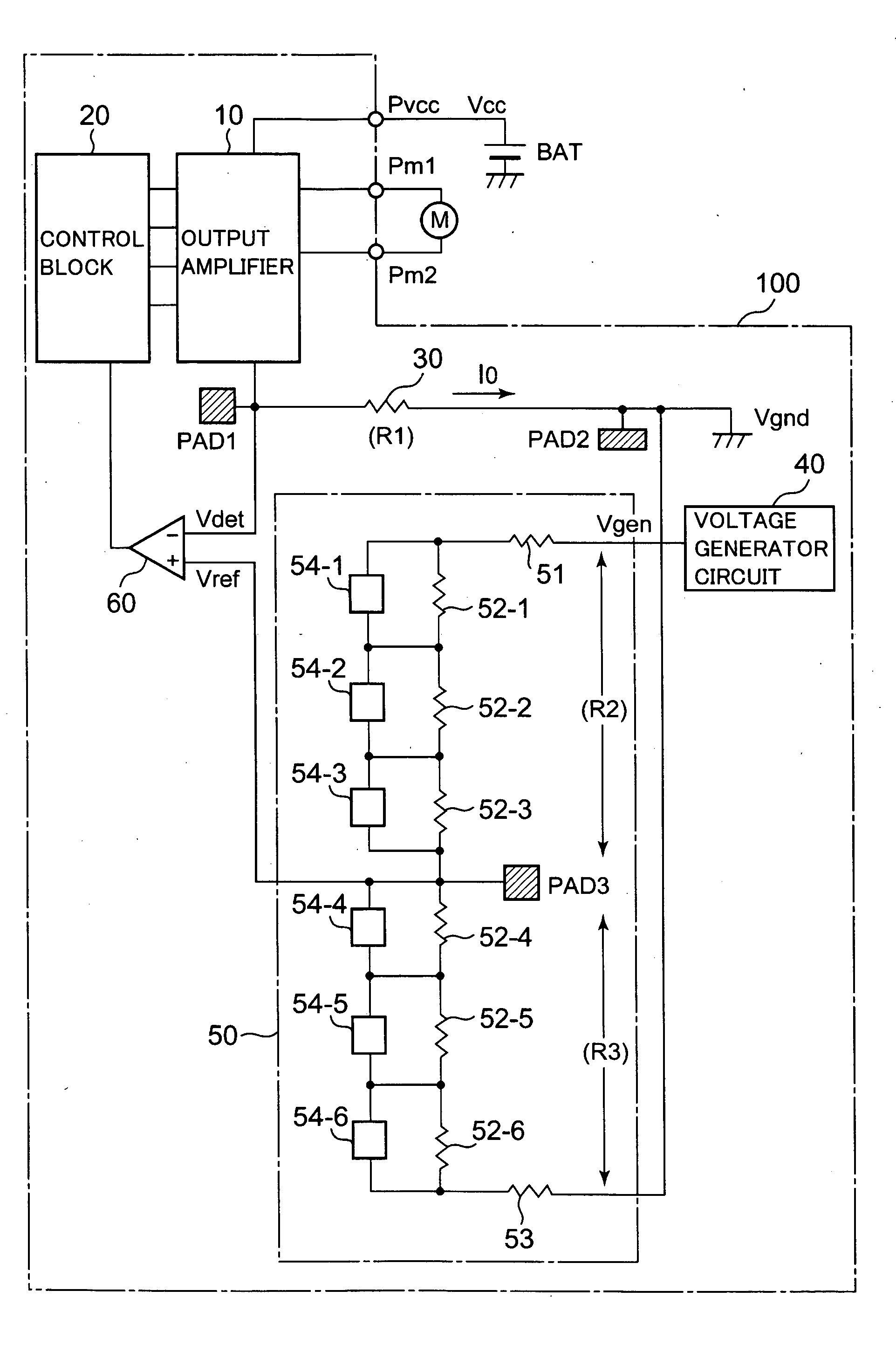
[0040]FIG. 1 shows a structure of a load-driving semiconductor device according to the present invention.

[0041] In FIG. 1, a supply voltage Vcc is input from a battery power supply BAT to a load-driving semiconductor device 100 via a power supply input terminal Pvcc. From load-driving semiconductor device 100, an output voltage and an output current are supplied to a motor M, which serves as a load, via output terminals Pm1 and Pm2.

[0042] An output amplifier 10 includes, for example, an output transistor circuit using a transistor. The output transistor circuit is controlled in accordance with a control signal coming from a control block 20. Via the transistor circuit controlled in accordance with the control signal, the output current is supplied from output amplifier 10 to motor M. The output current Io passes through a detecting resistor 30 to flow into a ground voltage Vgnd. Since a resistance value of detecting resistor 30 is represented as R1, a detected voltage Vdet is repre...

second embodiment

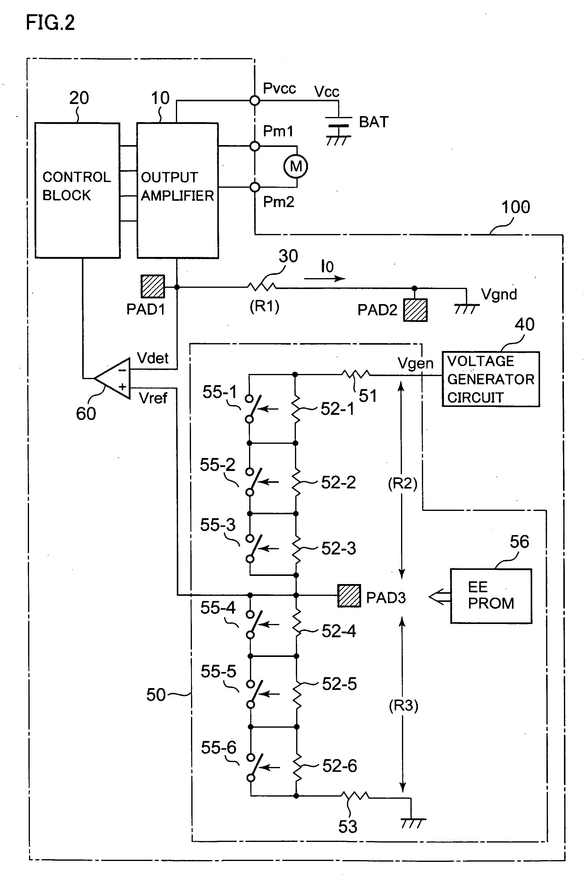
[0060]FIG. 2 shows a structure of a load-driving semiconductor device according to the present invention. In FIG. 2, switches 55-1 to 55-6 are used instead of the disconnectably configured connecting portions of trimming circuit 50 in FIG. 1, namely, fuses 54-1 to 54-6. A non-volatile storage 56 is provided to serve as a switch control circuit for storing information for setting switches 55-1 to 55-6 to an on or off state and controlling them. For switches 55-1 to 55-6, a MOS transistor, a bipolar transistor and the like can be used. For nonvolatile storage 56, an Electrically Erasable and Programmable Read Only Memory (EEPROM), a Ferroelectric Random Access Memory (FeRAM) and the like can be used.

[0061] Nonvolatile storage 56 stores information for controlling switches 55-1 to 55-6 to an on or off state for trimming in accordance with the measured resistance value of detecting resistor 30 as in the process of trimming reference voltage Vref in FIG. 1. Each of switches 55-1 to 55-6 ...

third embodiment

[0062]FIG. 3 shows a structure of a load-driving semiconductor device according to the present invention, providing a more specific structure of control block 20 and output amplifier 10 in FIGS. 1 and 2.

[0063] In FIG. 3, trimming circuit 50 is shown to have two components, namely, adjustable resistors (their resistance values are represented as R2 and R3).

[0064] Generated voltage Vgen from voltage generator circuit 40 is converted by a voltage converter circuit 41 and supplied to trimming circuit 50. In this example, voltage converter circuit 41 is composed of a 6-bit D / A converter 42 and a voltage follower 43. Generated voltage Vgen is converted to a prescribed voltage in accordance with a digital command signal Din input to D / A converter 42, and then output from voltage converter circuit 41.

[0065] By providing voltage converter circuit 41, a voltage can be adjusted (trimmed) not only in trimming circuit 50 but by digital command signal Din. Therefore, reference voltage Vref can ...


PUM


Abstract

In a load-driving semiconductor device, a part of metal interconnection in a metal interconnection layer is used to form a detecting resistor for detecting an output current, and a resistance-measuring pad for measuring a resistance value of the detecting resistor is provided. The load-driving semiconductor device generates a trimmed reference voltage in accordance with the resistance value of the detecting resistor, and controls drive of a load based on a comparison between the reference voltage and a detected voltage according to a voltage drop of the detecting resistor. Therefore, it is possible to provide a load-driving semiconductor device in which a current-detecting resistor for detecting a current that flows through a load is embedded to reduce space required on a substrate and thus reduce cost, and a current can be detected with high accuracy.

Description

BACKGROUND OF THE INVENTION [0001] 1. Field of the Invention [0002] The present invention relates to a load-driving semiconductor device that detects a current flowing through a load such as a motor to drive the load. [0003] 2. Description of the Background Art [0004] In a load-driving device for driving a load such as a motor, a load current flowing through the load has conventionally been detected to control or limit the current or control a torque by using a semiconductor device (IC) for driving a load. To detect the load current, a discrete (external) current-detecting resistor is provided to utilize its voltage drop to detect the amount of load current (Japanese Patent Laying-Open No. 2003-209993). [0005] The resistance value of the detecting resistor is usually set to be considerably low (e.g. approximately 0.1-0.5 Ω) to apply a sufficient voltage to the load and reduce a loss caused by the detecting resistor itself. The size of the current-detecting resistor is quite large, w...

Claims


Application Information

Patent Timeline
Patent Type & Authority Applications(United States)
IPC IPC(8): H03K5/153H02P29/00
CPCH02M2001/0009H03K17/6871H03K17/0822H02M1/0009
Inventor NAKAI, TATSUJIKUWAMURA, MAKOTO
Owner ROHM CO LTD
Why Eureka
Try Eureka