Bonded SOI substrate, and method for manufacturing the same

Active Publication Date: 2006-03-16
SUMCO CORP
View PDF2 Cites 43 Cited by
  • Summary
  • Abstract
  • Description
  • Claims
  • Application Information

AI Technical Summary

Benefits of technology

[0025] The present invention aims to provide a bonded SOI substrate which can perform gettering of metallic impurities in the SOI layer during thermal processing in a device process, and a method for manufacturing the same.
[0026] Also, the present invention aims to provide a method for manufacturing a bonded SOI substrate which can perform gettering of metallic contaminants which contaminated a surface layer of the wafer for an active layer during ion implantation.
[0027] Furthermore,

Problems solved by technology

Furthermore, as a specific problem for bonded SOI substrates accompanying ion implantation, metallic contamination is caused in an ion implantation process and a subsequent high temperature heat-treating process (for example, thermal oxidation or heat-treating for bonding).
This problem also occurs in the case in which metallic contamination is caused in the device process.
As a result, a yield rate for the devices drops.
However, according to such a prior art method for manufacturing a bonded SOI substrate, since the IG layer is formed in the wafer for a support substrate in this manner, iron, nickel, or the like in the SOI layer, of which diffusion rates in the buried oxide film

Method used


Image

  • Bonded SOI substrate, and method for manufacturing the same
  • Bonded SOI substrate, and method for manufacturing the same
  • Bonded SOI substrate, and method for manufacturing the same

Examples


example 1

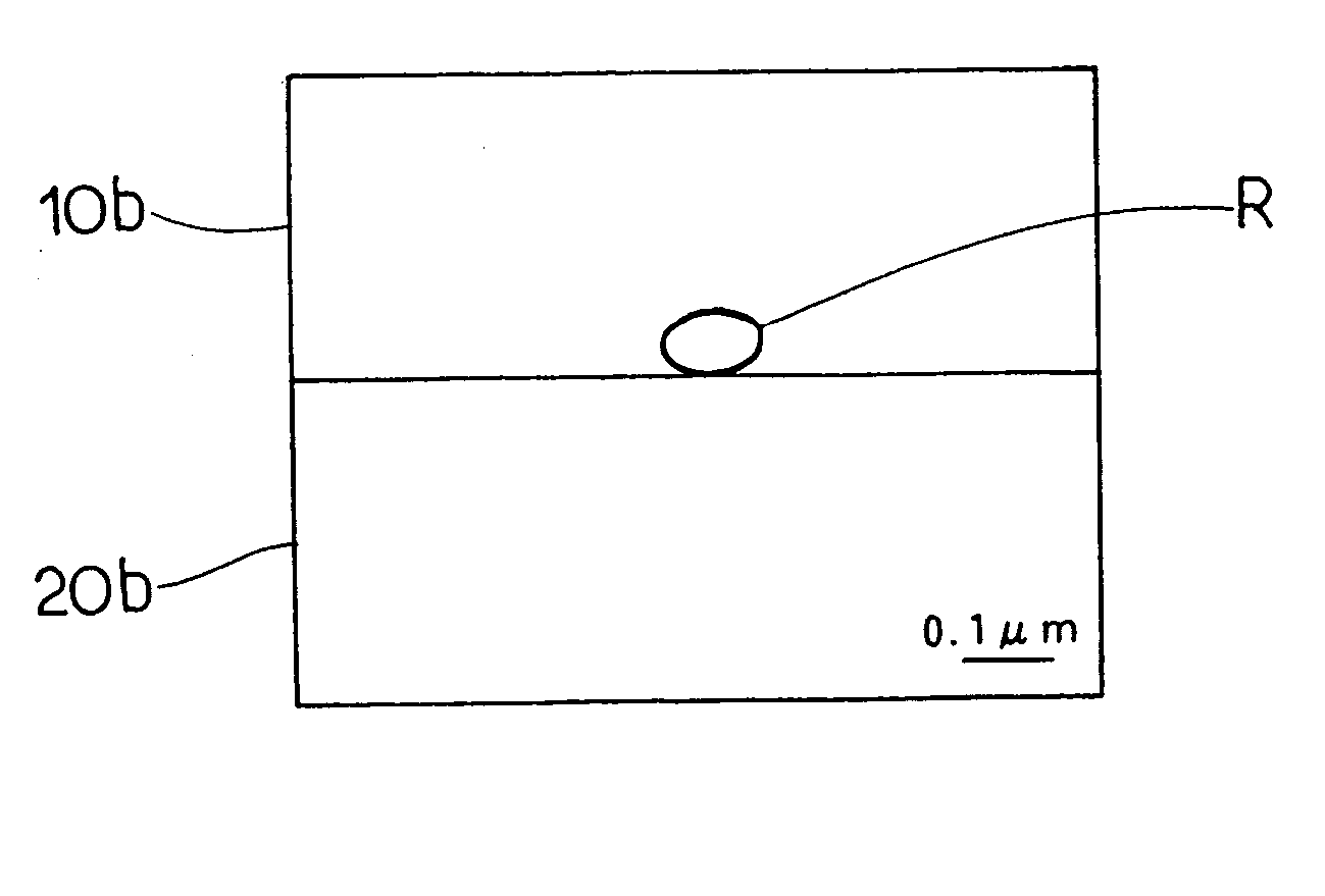
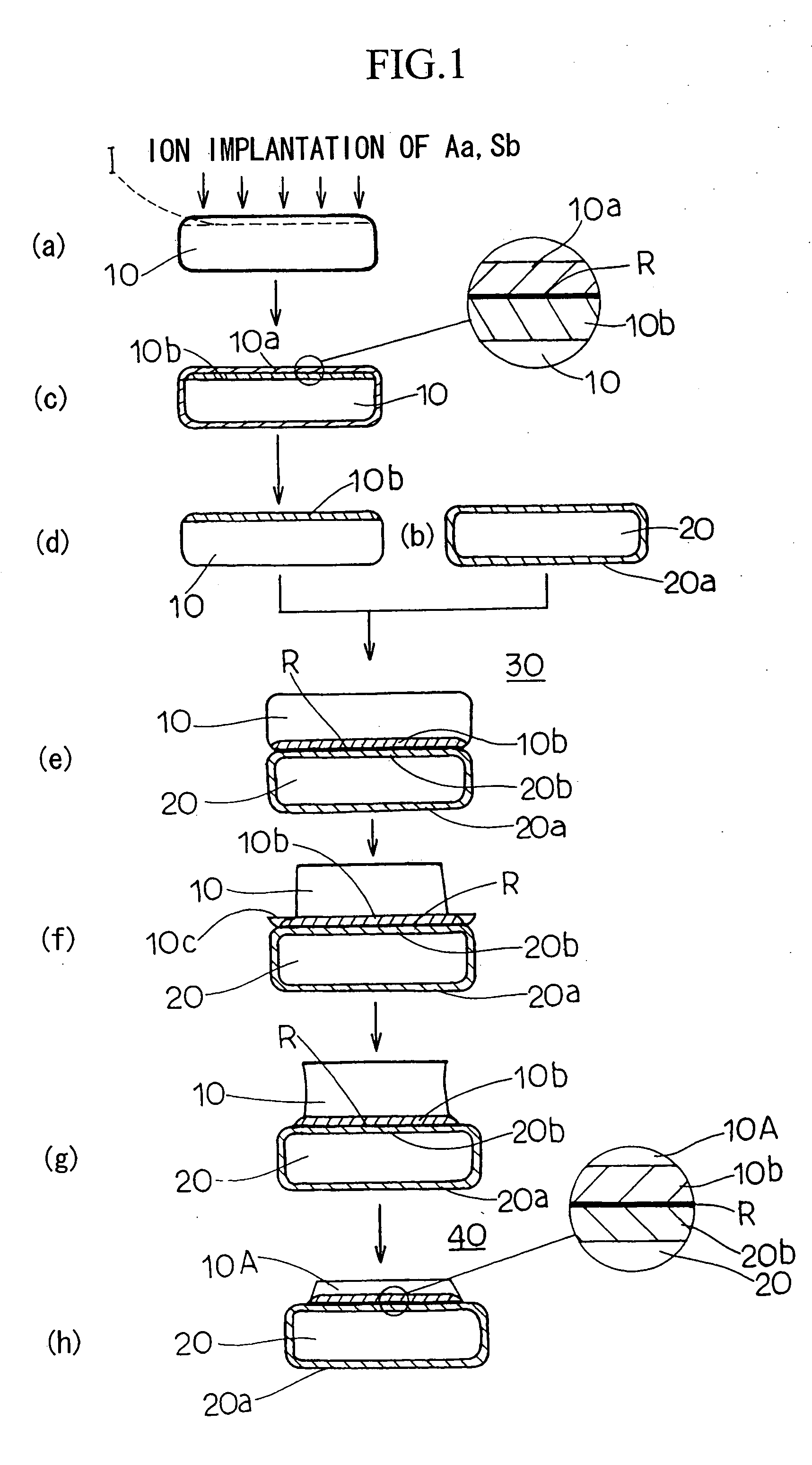
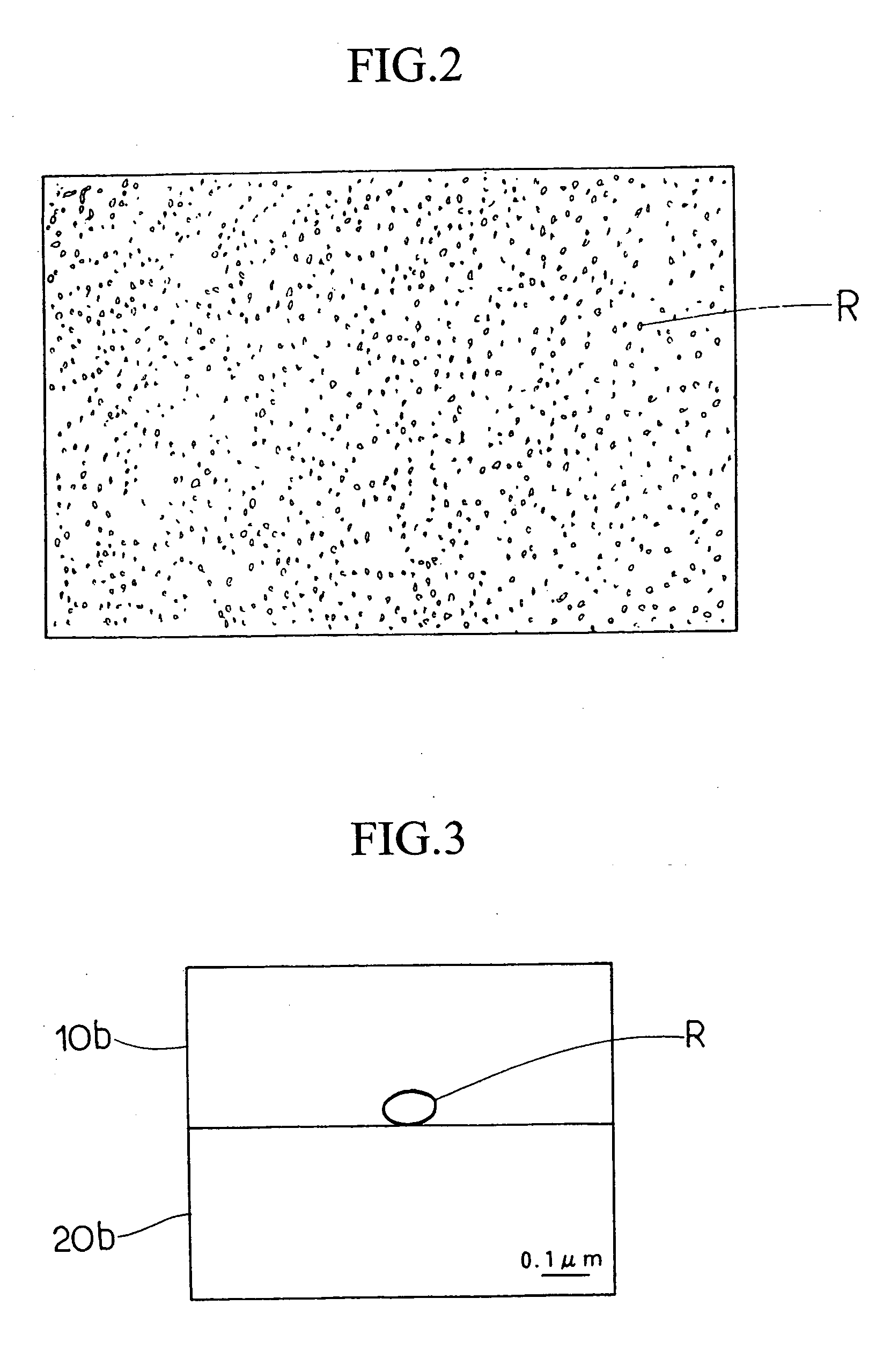
[0098] As shown in FIG. 1, a single crystal silicon ingot doped with a predetermined amount of arsenic or antimony is pulled up by the CZ method (alternatively, the FZ method may be applied). And then, the obtained single crystal silicon ingot is subjected to block cutting, a notching process, slicing, chamfering, mirror polishing of a surface, and the like. Thereby, a mirror-polished n-type wafer for an active layer 10 of 8 inches in diameter is prepared (see FIG. 1(a)). In contrast, a similar mirror-polished wafer for a support substrate 20 is prepared by the same manufacturing process as for the wafer for an active layer 10 (see FIG. 1(b)). Next, the wafer for the support substrate 20 is put into a thermal oxidization furnace, and is subjected to a thermal oxidization process in an atmosphere of water vapor at a temperature of 1050° C. for four hours. Thereby, a silicon oxide film (an insulating film) 20a having a thickness of 1.0 μm is formed.

[0099] Next, from a surface of the ...

example 2

[0113] Next, referring to FIG. 4, a bonded SOI substrate and a method for manufacturing the same of Example 2 of the present invention will be explained below.

[0114] As shown in FIG. 4, a non-doped single crystal silicon ingot is pulled up by the CZ method. And then, the obtained single crystal silicon ingot is subjected to block cutting, a notching process, slicing, chamfering, mirror polishing of a surface, and the like. Thereby, a mirror-polished non-doped wafer for an active layer 10 of 8 inches in diameter is prepared (see FIG. 4(a)). In contarst, a similar mirror-polished wafer 20 for a support substrate is prepared by the same manufacturing process as for the wafer for an active layer 10 (see FIG. 4(b)).

[0115] Next, from a surface of the wafer for an active layer 10, arsenic or antimony is implanted at, for example, an implantation energy of 60 keV and a dose amount of 1×10¹⁵ atoms / cm2. Thereby, an ion implantation layer I is formed at a predetermined depth in a surface lay...


PUM


Abstract

This bonded SOI substrate includes: an SOI layer having a low density impurity layer in which dopants are present at low density and a high density impurity layer in which dopants are present at high density; a wafer for a support substrate which supports said SOI layer; and a buried insulating film, wherein said SOI layer and said wafer for a support substrate are bonded with said buried insulating film therebetween, and gettering sites are formed in said high density impurity layer.

Description

BACKGROUND OF THE INVENTION [0001] 1. Field of the Invention [0002] The present invention relates to a bonded SOI substrate and a method for manufacturing the same, and more particularly it relates to a bonded SOI substrate in which gettering sites are formed in an SOI layer, and a method for manufacturing the same. [0003] This application claims priority from Japanese Patent Application No. 2004-149707 filed on May 19, 2004, the content of which is incorporated herein by reference. [0004] 2. Background Art [0005] As one example of bonded substrates in which two silicon wafers are bonded together, a bonded SOI (Silicon On Insulator) substrate is known. This includes an SOI layer (an active layer) on a surface of which a device is formed, a wafer for a support substrate which supports the active layer from its rear surface, and an insulating film (a silicon oxide film) buried therebetween. In the prior art, there has also been disclosed a bonded SOI substrate in which a high density ...

Claims


Application Information

Patent Timeline
IPC IPC(8): H01L23/58
CPCH01L21/26513H01L2924/01033H01L21/3226H01L21/76256H01L21/84H01L24/26H01L24/83H01L2224/16H01L2224/83099H01L2224/8385H01L2224/83894H01L2924/01005H01L2924/01013H01L2924/01015H01L2924/01027H01L2924/01029H01L2924/01051H01L2924/07802H01L2924/01006H01L2924/01021H01L21/3221
Inventor TOMITA, SHINICHITSUTSUMI, MASAHIDE
Owner SUMCO CORP
Why Eureka
Try Eureka