Semiconductor device and method of fabricating a ltps film

a low-temperature polysilicon, semiconductor technology, applied in the direction of semiconductor devices, electrical equipment, transistors, etc., can solve the problems of affecting the electrical performance affecting the uniformity of the semiconductor device, and affecting the mobility of the carrier. the effect of uniformity and mobility of the carrier

Inactive Publication Date: 2006-03-23
AU OPTRONICS CORP
View PDF7 Cites 29 Cited by
  • Summary
  • Abstract
  • Description
  • Claims
  • Application Information

AI Technical Summary

Benefits of technology

[0013] It is an advantage of the present invention that the laser absorption layer and the insulating layer are utilized to cover portions of the amorphous silicon film and make the covered portions of the amorphous silicon film get rid of laser irradiation. A temperature gradient occurs between the portions of the amorphous silicon film without laser irradiation and the portions of the amorphous silicon film with laser irradiation. This temperature gradient induces a lateral growth of silicon grains from the region without laser irradiation toward the region with laser irradiation. Accordingly, the present invention controls the numbers of grains and grain boundaries in the channel region via the pattern definition of the laser absorption layer and the insulating layer. Since it is achievable to form bigger grain sizes with only one grain boundary in the channel region, the carrier mobility and uniformity of TFTs can be improved, and a better electrical performance of the semiconductor device can be provided.
[0014] These and other objects of the claimed invention will be apparent to those of ordinary skill in the art with reference to the following detailed description of the preferred embodiments illustrated in the various drawings.

Problems solved by technology

Although this method produces grain sizes much bigger than the conventional grain sizes, it can't control the numbers of grains and grain boundaries in the channel region of the device.
As a result, noticeable difference of electrical characteristics in the transistor is produced.
The method controls the silicon grains to uniformly grow along a lateral direction, however, damage to the uniformity is caused during the etching process and different thicknesses of the amorphous silicon film at different locations will affect the activation process.

Method used


Image

  • Semiconductor device and method of fabricating a ltps film
  • Semiconductor device and method of fabricating a ltps film
  • Semiconductor device and method of fabricating a ltps film

Examples


Embodiment Construction

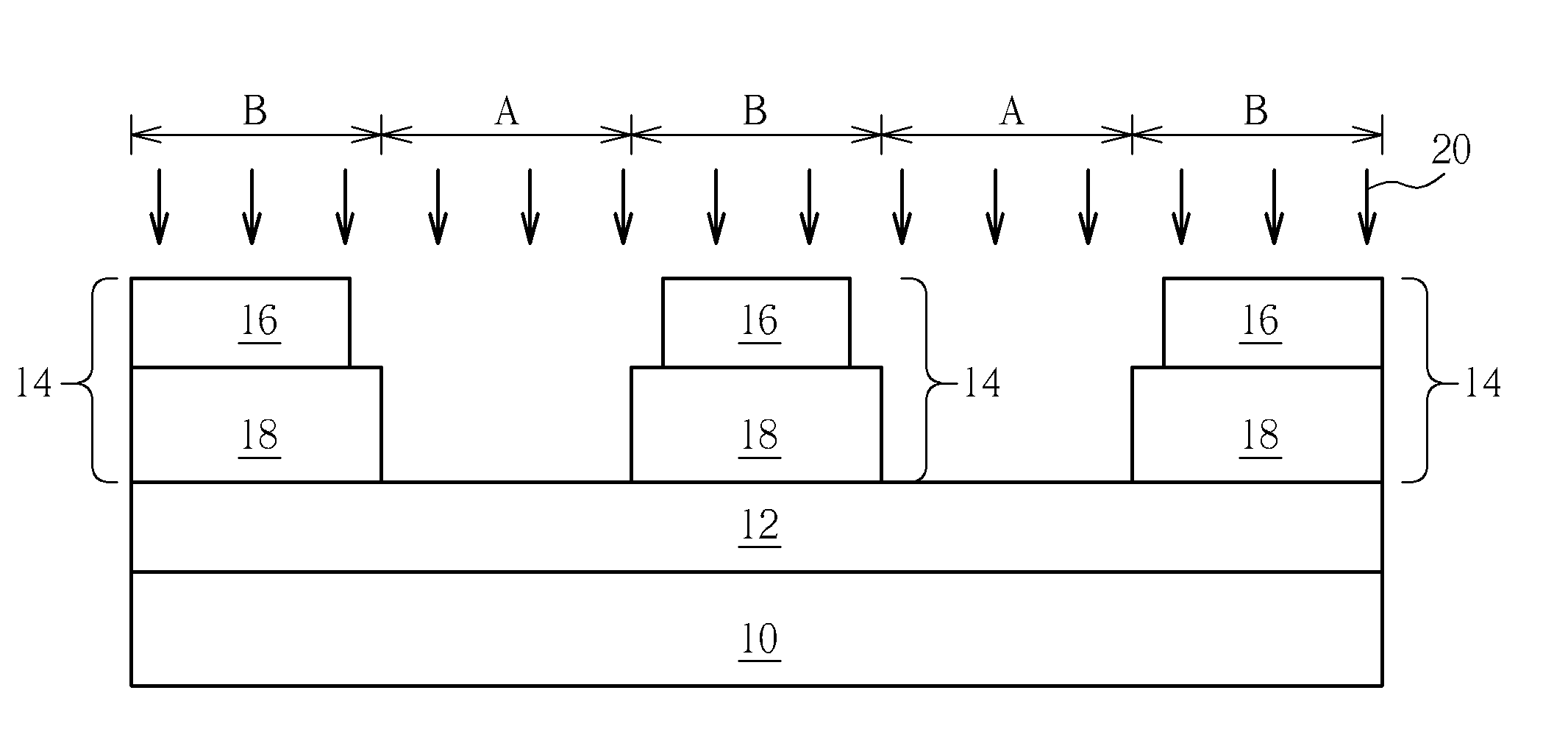
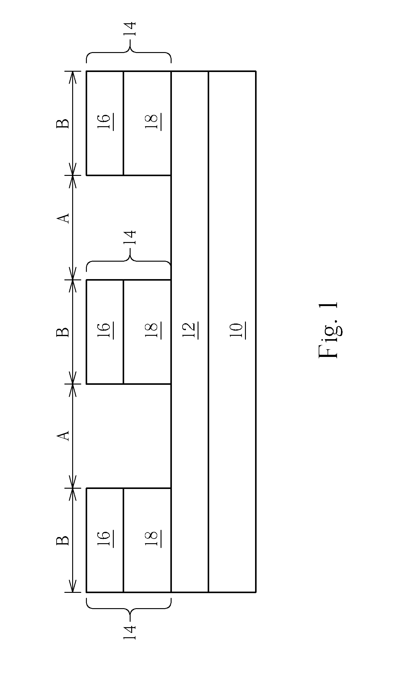
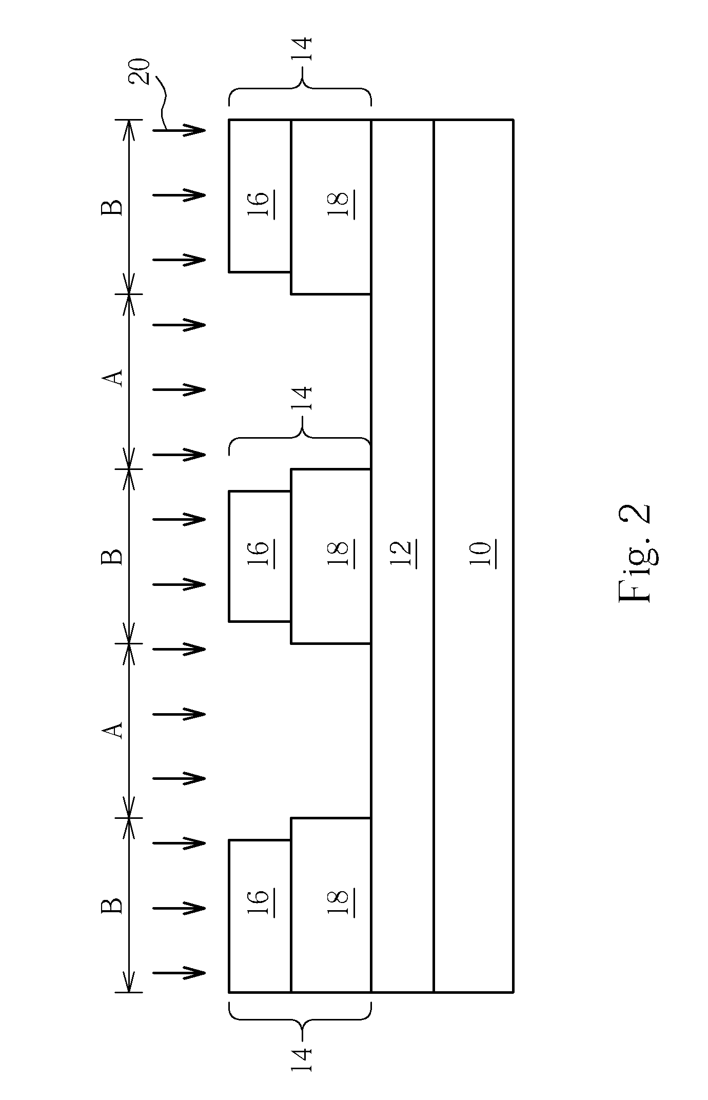
[0020] Referring to FIGS. 1 and 2, FIGS. 1 and 2 are schematic diagrams of a method of fabricating an LTPS film according to the present invention. As shown in FIG. 1, a substrate 10, such as a glass substrate, a quartz substrate, or a plastic substrate, is provided. An amorphous silicon film 12 is formed on the substrate 10, and a laser isolation pattern 14, which is composed of a laser absorption layer 16 and an insulating layer 18, is formed to cover portions of the amorphous silicon film 12. For example, a plasma enhanced chemical vapor deposition (PECVD) is used to continuously deposit the amorphous silicon film 12, the insulating layer 18 and the laser absorption layer 16 on the substrate 10. At least one channel region A and at least one non-channel region B surrounding the channel region A are defined in the amorphous silicon film 12. The laser absorption layer 16 can be formed of at least one material selected from amorphous silicon, polysilicon, metal oxide (including TiO2...


PUM

PropertyMeasurementUnit
temperatureaaaaaaaaaa

Abstract

A semiconductor device and a method of fabricating a low-temperature polysilicon film are provided. An amorphous silicon film is formed over a substrate. An insulating layer and a laser absorption layer are formed over the amorphous silicon film. A photolithographic and etching process is performed to remove portions of the laser absorption layer and the insulating layer to expose portions of the amorphous silicon film. A laser crystallization process is utilized to convert the amorphous silicon film into a polysilicon film.

Description

BACKGROUND OF INVENTION [0001] 1. Field of the Invention [0002] The present invention relates to a semiconductor device and a method of fabricating a low-temperature polysilicon (LTPS) film, and more particularly, to a semiconductor device and a method of fabricating a LTPS film utilizing lateral grain growth. [0003] 2. Description of the Prior Art [0004] In the process of fabricating thin-film transistor liquid crystal displays (TFT LCDs), glass deforms when exposed to temperature above 600° C., and the deposition temperature of a polysilicon film is required to between 575-650° C. In order to avoid deformation of the glass substrate at the high temperature for depositing the poly silicon film, a method of crystallizing an amorphous silicon layer has been gradually adopted in the present fabrication of LTPS films in TFT LCDs. [0005] A conventional LTPS film is fabricated on an insulating substrate, and the insulating substrate is made of materials pervious to light, such as a glass...

Claims


Application Information

Patent Timeline
Patent Type & Authority Applications(United States)
IPC IPC(8): H01L29/04H01L21/20H01L29/786
CPCH01L21/2026H01L21/02686H01L21/02422H01L21/02532H01L21/0242H01L21/02595H01L21/02675
Inventor CHANG, CHIH-HSIUNGCHEN, YI-WEISUN, MING-WEI
Owner AU OPTRONICS CORP
Why Eureka
Try Eureka