Cathode structure for field emission device

a cathode and emission device technology, applied in the direction of discharge tube/lamp details, nanoinformatics, discharge tube luminescnet screens, etc., can solve the problems of high redundant electron source for display, serious and possibly damaging design, etc., to reduce or eliminate electrical shorting, avoid or reduce arcing, and the driving of the device is made more stabl

Inactive Publication Date: 2006-03-30
ARROW CAPITAL +1
View PDF18 Cites 65 Cited by
  • Summary
  • Abstract
  • Description
  • Claims
  • Application Information

AI Technical Summary

Benefits of technology

[0011] In one embodiment, a bottom portion of the gate electrode is protected with a dielectric or other insulating material to avoid or reduce arcing from emitters to the gate electrode. This insulating material may further help to reduce or eliminate electrical shorting between the gate electrode and the emitters, which are electrically coupled to the emitter electrode. By reducing arcing, the driving of the device is made more stable, allowing the voltage applied to the gate electrode to be increased. Increasing the gate voltage increases the electron emission from the emitters, which results in a greater maximum brightness of picture elements in a display. As a result of reducing or eliminating electrical shorting, the gate leakage current is reduced. This allows for a higher anode current under the same operating conditions, which also leads to a greater maximum brightness of picture elements in a display.
[0012] In one embodiment, a method for manufacturing a field emission de...

Problems solved by technology

This provides a highly redundant electron source for the display.
A problem arises in the design of such displays, however, due to their use of electric fields between the emitters and the other electrodes.
The electric fields involved in these field emission displays can cause electrical arcing between the electrodes (e.g. the gate electrode and the emitter electrode, of the emitters thereon), which can result in serious and possibly damaging results.
When arcing occurs, the electrodes may be compromised.
The gate electrode, for example, can be partially melted, and the hole structure in which the emitters are disposed can be...

Method used


Image

  • Cathode structure for field emission device
  • Cathode structure for field emission device
  • Cathode structure for field emission device

Examples


Embodiment Construction

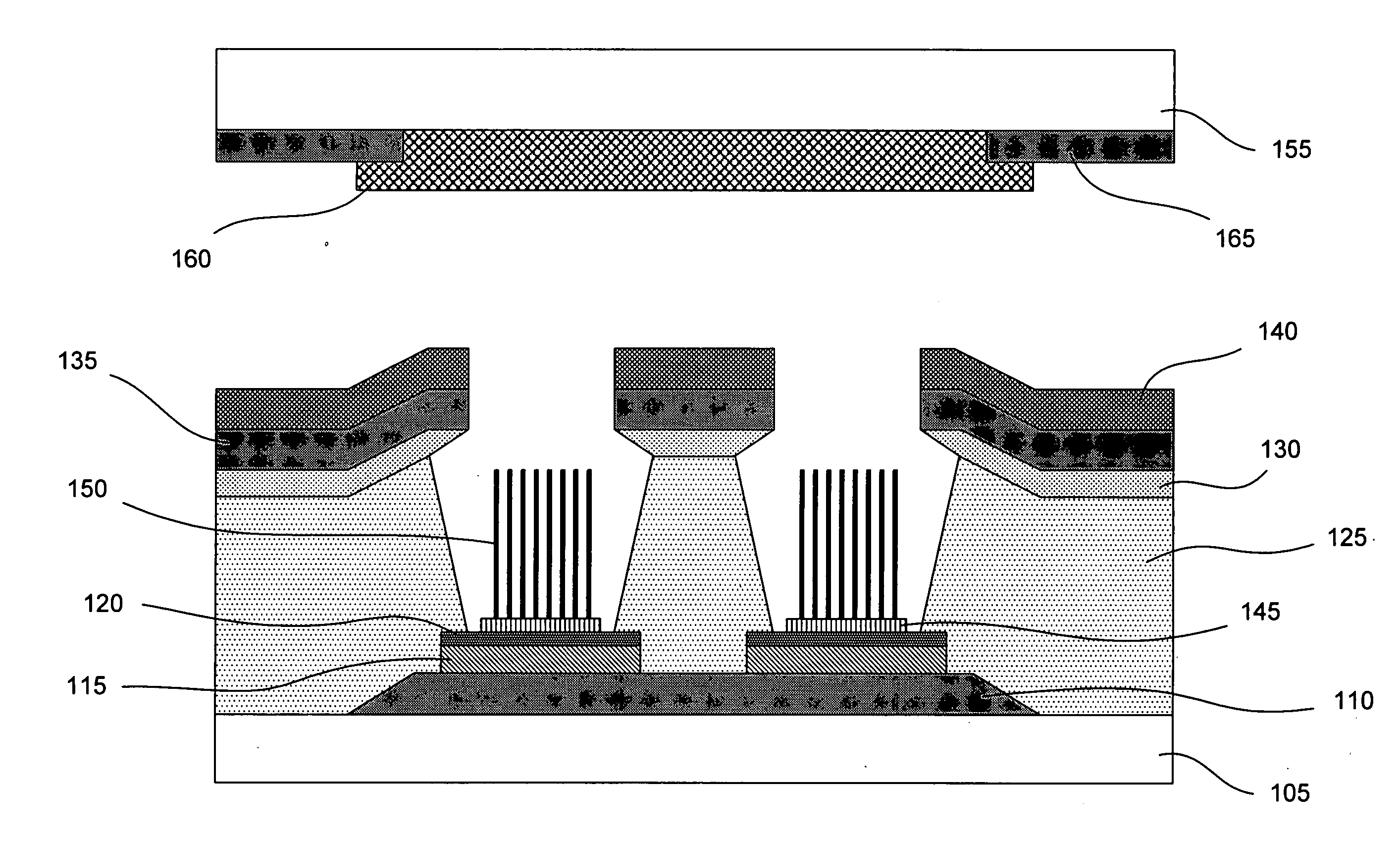
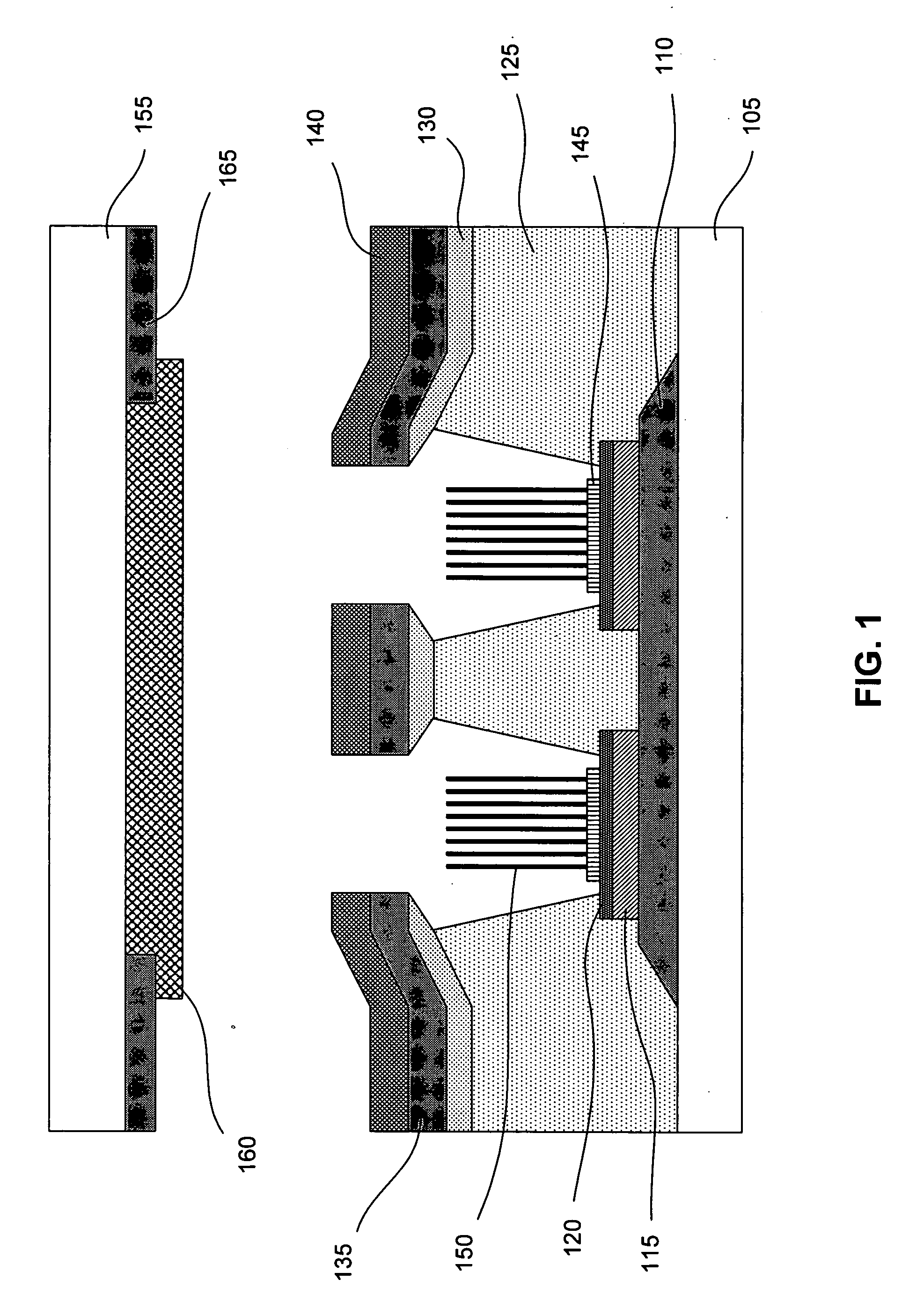
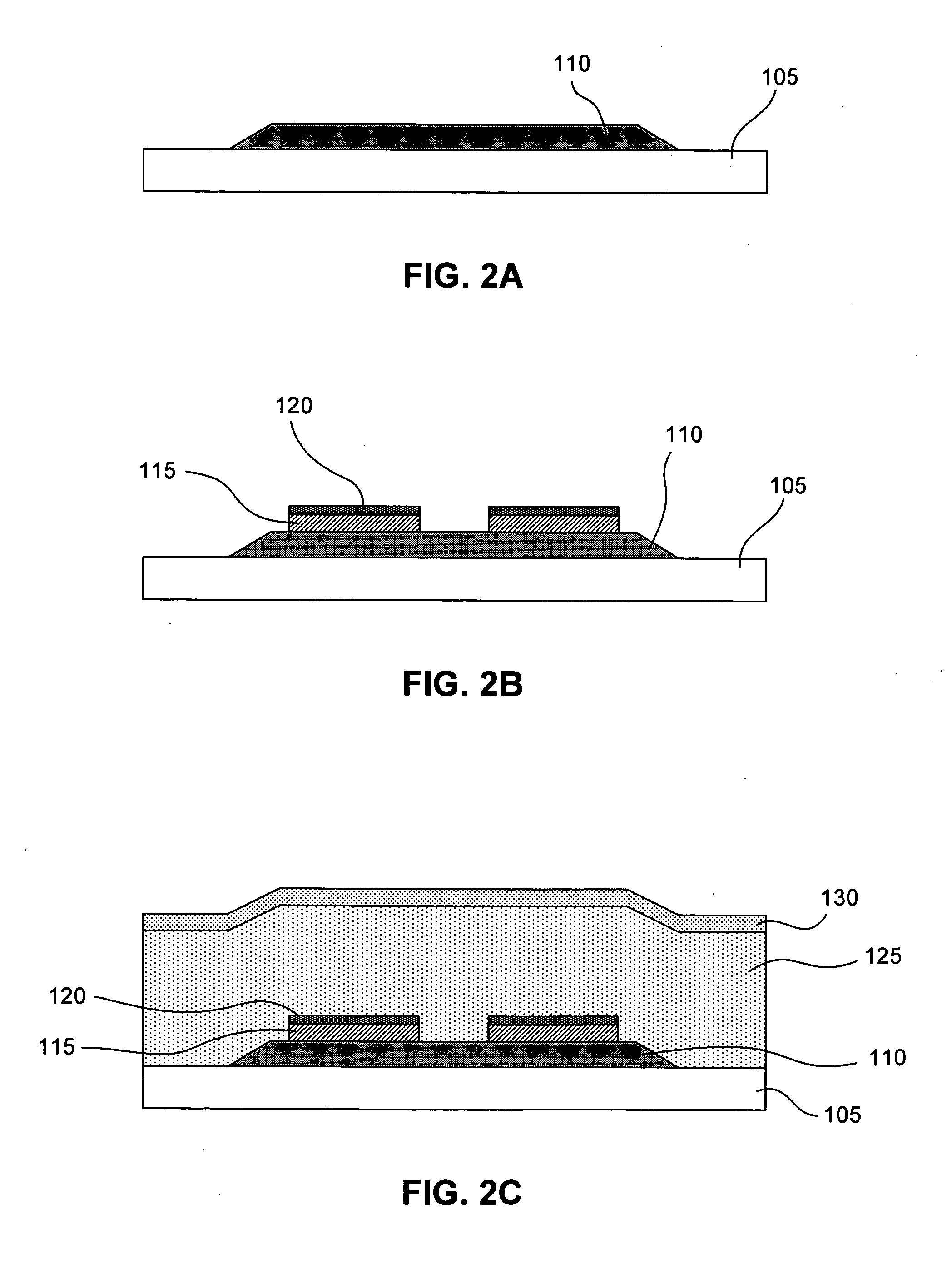
[0016]FIG. 1 illustrates one embodiment of a field emission device for emitting electrons, such as a portion of a CNT-based field emission display described above. The field emission device shown in FIG. 1 comprises two main structures: a cathode structure and an anode structure. The cathode structure includes a number of layers of material deposited over a substrate 105, such as glass. In one embodiment, the layers of the cathode structure include an emitter electrode 110, a resistor layer 115, a barrier layer 120, one or more insulating layers 125 and 130, a gate electrode 135, and a passivation layer 140. The cathode structure further comprises electron emitters 150, such as carbon nanotubes, which are situated in one or more emitter holes formed through a portion of the cathode structure. Preferably, the electron emitters 150 are disposed on or in electrical coupling with the emitter electrode 110. The electron emitters may be formed from a catalyst layer 145, which rests over t...


PUM


Abstract

To avoid arcing and shorting within a field emission device, a bottom portion of a gate electrode is protected with an insulating material to avoid or reduce arcing among the electrodes and the electron emitters in the device. In a method for manufacturing such a field emission device, an emitter hole is formed through an insulating layer such that a portion of the gate electrode overhangs the hole and is protected on its underside by the insulating layer. The device can be used in display systems, such as CNT flat panel displays.

Description

BACKGROUND [0001] 1. Field of the Invention [0002] This invention relates generally to field emission devices, and in particular to cathode structures for field emission devices designed to avoid arcing and shorting among the electron emitters and the electrodes in the device. [0003] 2. Background of the Invention [0004] Flat panel displays (FPDs) using carbon nanotube (CNT) technology are replacing and superceding existing display technologies, including those that use cathode ray tubes (CRTs), thin film transistor liquid crystals (TFT-LCDs), plasma display panels (PDPs), and organic light emitting diodes (OLEDs). The emerging CNT-based flat panel display technology uses a process for generating pictures similar to the method used in CRTs. But instead of a CRT's single hot filament electron gun, CNT-based displays use a planar array of carbon nanotube emitters as a source of electrons. [0005] In one example, a CNT-based field emission display comprises a cathode structure disposed ...

Claims


Application Information

Patent Timeline
IPC IPC(8): H01J1/62
CPCB82Y10/00H01J31/127H01J29/481H01J3/021
Inventor SON, JONG WOO
Owner ARROW CAPITAL
Why Eureka
Try Eureka