High voltage MOS transistor with up-retro well

a high-voltage mos transistor and up-retro well technology, which is applied in the direction of semiconductor devices, semiconductor/solid-state device details, electrical apparatus, etc., can solve the problems of increasing the electric field under the gate, undesired current flow between the drain and the buried layer, and the dmos transistor b>10/b> to have undesired large device dimensions, etc., to achieve the effect of low threshold voltag

Inactive Publication Date: 2006-04-06
ANALOG DEVICES INT UNLTD
View PDF7 Cites 21 Cited by
  • Summary
  • Abstract
  • Description
  • Claims
  • Application Information

AI Technical Summary

Benefits of technology

[0014] It is an object of the present to provide an MOS transistor that has a thin epitaxial layer and can operate at high voltages without experiencing vertical punch-through or breakdown.
[0019] The up-retro well prevents vertical punch-through and breakdown, and allows for a low threshold voltage in high voltage MOS transistors. High voltage MOS transistors with an up-retro well may be formed in a semiconductor wafer that has a thin epitaxial layer. Also, high voltage MOS transistors of the present invention can be used as pass transistors because the source and drain regions may be used interchangeably. High-voltage MOS transistors of the present invention may be fabricated using processes that are standard in low voltage sub-micron CMOS and BiCMOS process technology.

Problems solved by technology

Applying a high voltage to a transistor can cause several problems.
Vertical punch-through can cause unwanted current flow between the drain and the buried layer at high drain voltages.
However, thick oxide layer 18 causes DMOS transistor 10 to have undesirably large device dimensions.
A further disadvantage of transistor 10 is that the N-type doping concentration in N-type drain region 13 is higher near bird's beak 18A of thick oxide 18 than the N-type doping concentration near the lower boundary 18B of thick oxide 18.
This effect causes an increased electric field under the gate which is also undesirable.
A further disadvantage of DMOS transistor 10 is that it cannot be used as a pass transistor, particularly a high voltage pass transistor.
Furthermore, in a high voltage pass transistor, the body region cannot be tied electrically to either the source or the drain.
Therefore, the output capacitance at the drain is undesirably high because N+ buried layer 28 has a wide area.
High output capacitance is undesirable because it slows down the frequency of the transistor's output signal.
High doping in body region 35 causes the undesirable effects of increasing the threshold voltage of the transistor and reducing the breakdown voltage at the drain-to-body junction.
However, the reduction in the P-type doping concentration at the surface of the retrograde well is typically not adequate to achieve the desired reduction in surface concentration to achieve a sufficient reduction in the threshold voltage and protection against vertical punch-through.
These tools are not commonly available and are extremely expensive.

Method used


Image

  • High voltage MOS transistor with up-retro well
  • High voltage MOS transistor with up-retro well
  • High voltage MOS transistor with up-retro well

Examples


Embodiment Construction

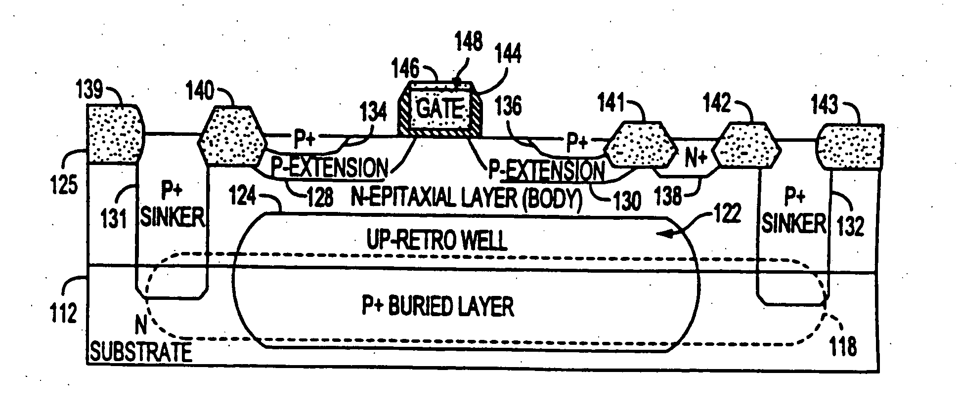
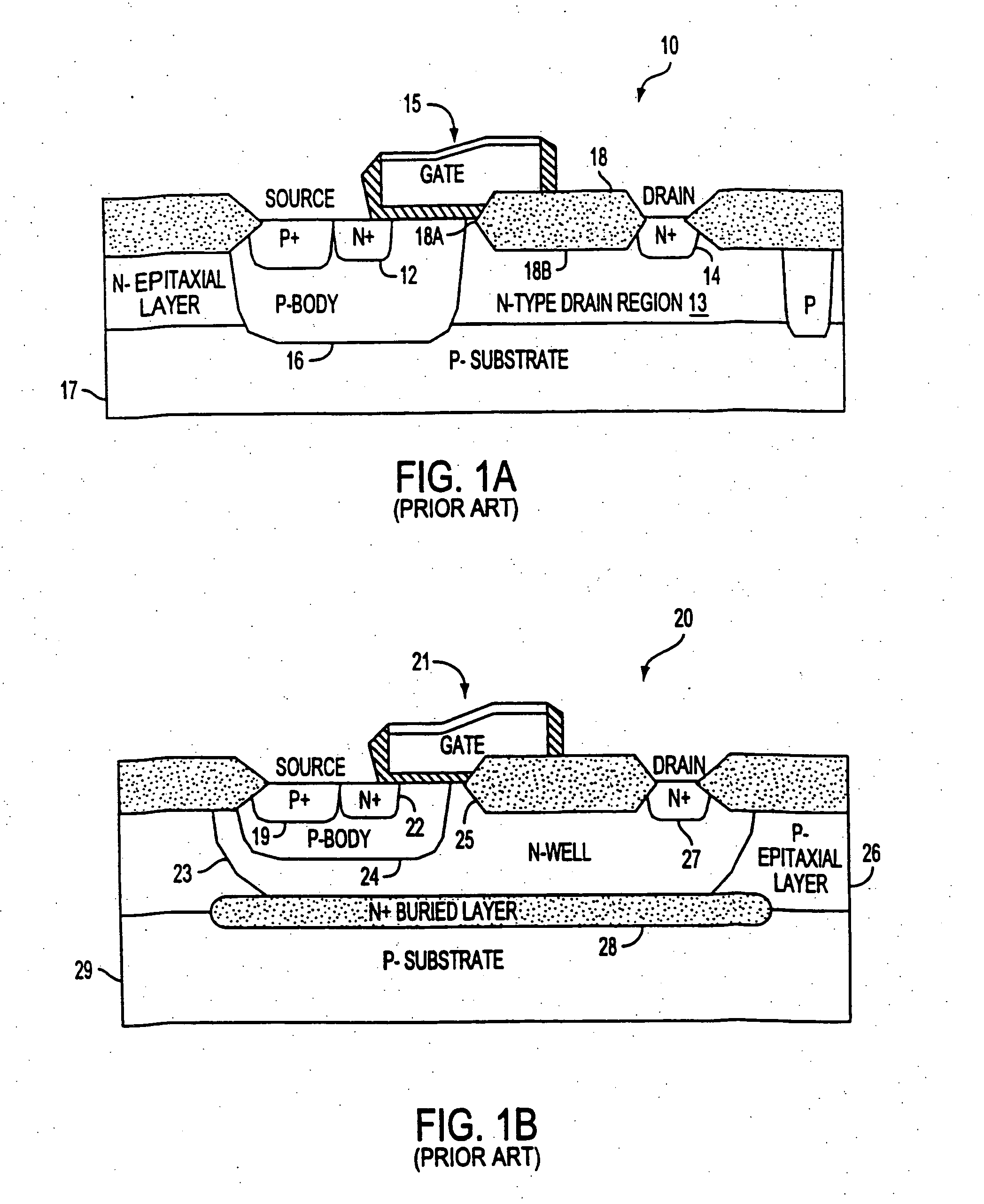
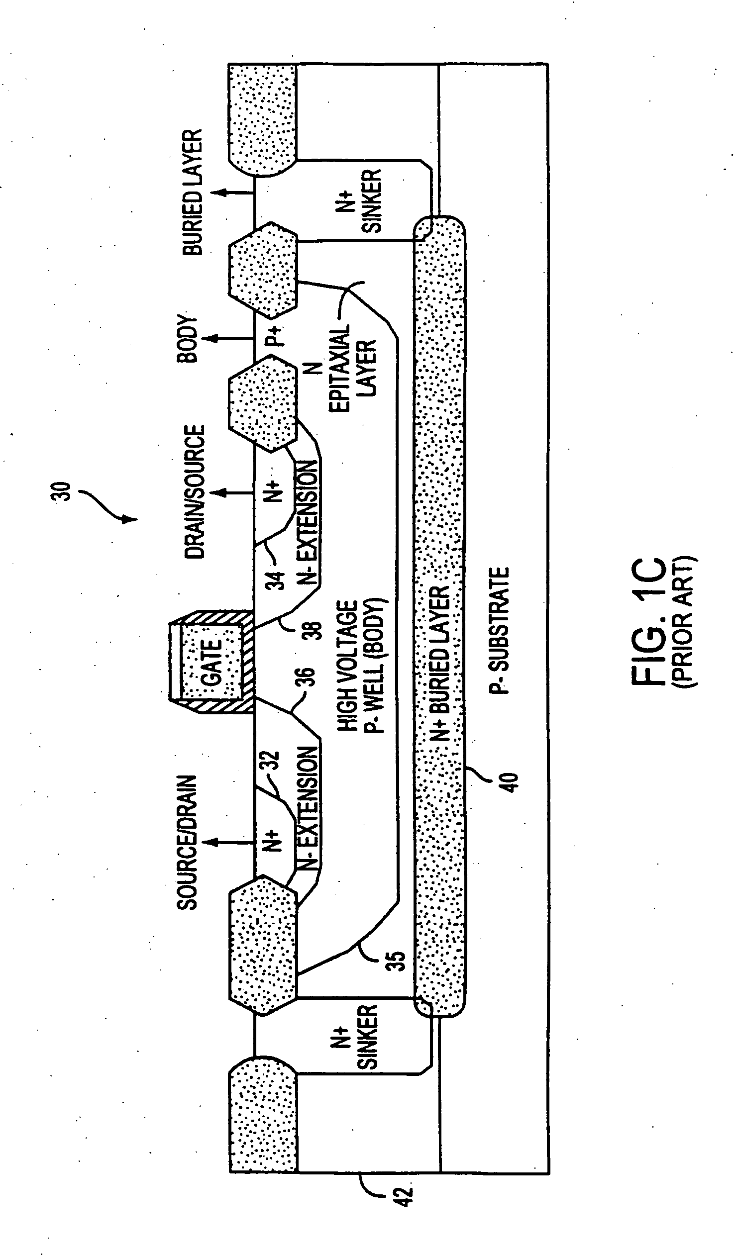
[0034] Process steps for an illustrative embodiment of a high voltage MOS transistor with an up-retro well are shown in FIGS. 3A-3F. In this embodiment, an NMOS transistor is formed in a P-type epitaxial layer on a P-type substrate. A highly doped N+ buried layer is formed in the P-substrate to isolate the P-epitaxial layer and the P-substrate. The NMOS transistor has a P-type up-retro well that is formed from dopants implanted into the substrate. The up-retro well P-type dopants diffuse into the P-epitaxial layer (farther than the N-type buried layer dopants) when the epitaxial layer is formed and during subsequent heating steps. The P-type up-retro well dopants increase the net concentration of P-type dopants in the region of the P-epitaxial layer into which the up-retro well dopants diffuse. The region of increased net P-type doping concentration is above the epitaxy-substrate interface. The up-retro well dopants allow the epitaxial layer to be made relatively thin. The increased...


PUM


Abstract

A high voltage MOS transistor is provided that is compatible with low-voltage, sub-micron CMOS and BiCMOS processes. The high voltage transistor of the present invention has dopants that are implanted into the substrate prior to formation of the epitaxial layer. The implanted dopants diffuse into the epitaxial layer from the substrate during the formation of the epitaxial layer and subsequent heating steps. The implanted dopants increase the doping concentration in a lower portion of the epitaxial layer. The implanted dopants may diffuse father into the epitaxial layer than dopants in the buried layer forming an up-retro well that prevents vertical punch-through at high operating voltages for thin epitaxial layers. In addition, the doping concentration below the gate may be light so that the threshold voltage of the transistor is low. Also, the high voltage transistor of the present invention may be isolated from the substrate and the buried layer, and have symmetrical source and drain regions so that it can be used as a pass transistor.

Description

CROSS REFERENCE TO RELATED APPLICATION [0001] This is a divisional of commonly-assigned U.S. patent application Ser. No. 10 / 858,619 filed on Jun. 1, 2004, which is continuation of commonly-assigned U.S. patent application Ser. No. 10 / 345,467 filed Jan. 14, 2003, which issued as U.S. Pat. No. 6,768,173 on Jun. 27, 2004, which is a divisional of commonly-assigned U.S. patent application Ser. No. 09 / 564,597 filed May 3, 2000, which issued as U.S. Pat. No. 6,528,850 on Mar. 4, 2003.BACKGROUND OF THE INVENTION [0002] This invention relates to high voltage MOS transistors. More particularly, this invention relates to apparatus and methods for forming an MOS transistor with a substrate implant to achieve various combinations of low threshold voltage, high breakdown voltage, and transistor operation at high voltages without experiencing vertical punch-through. [0003] Many applications for semiconductor devices require transistors that are isolated from the substrate and that can operate at ...

Claims


Application Information

Patent Timeline
Patent Type & Authority Applications(United States)
IPC IPC(8): H01L29/76H01L21/336H01L21/8249H01L27/06H01L29/10H01L29/78
CPCH01L21/26513H01L21/8249H01L27/0623H01L29/1083H01L29/7833H01L21/2658
Inventor HEBERT, FRANCOIS
Owner ANALOG DEVICES INT UNLTD
Why Eureka
Try Eureka