Semiconductor device

a semiconductor device and semiconductor technology, applied in the direction of pulse generators, pulse techniques, machines/engines, etc., can solve the problems of complex circuit configuration and adjustment, output current is not linearly proportional, and the characteristics of the semiconductor device itself or load are degraded or broken, etc., to achieve the effect of simple circuit configuration

Active Publication Date: 2006-04-13
MITSUBISHI ELECTRIC CORP
View PDF5 Cites 37 Cited by
  • Summary
  • Abstract
  • Description
  • Claims
  • Application Information

AI Technical Summary

Benefits of technology

[0011] It is an object of the present invention to provide a technique of controlling an induced electromotive force generated in an inductive load when forcedly interrupting a switching device, with a simple circuit configuration.

Problems solved by technology

An ignition system for an internal combustion engine such as an automobile engine has a problem in that a control signal is held “on” due to a misoperation or the like during maintenance, causing a switching device for controlling current in an inductive load (e.g., transformer or load coil) to be kept conducting, which results in degradation in characteristics or breakdown of a semiconductor device itself or load due to heat generation.
In this case, a forced current interruption in the switching device may generate a great induced electromotive force in an inductive load, causing arc discharge to take place in an ignition coil with timing that a computer for controlling the ignition of an internal combustion engine is not intended to follow.
Generally, however, output current is not linearly proportional to the gate voltage in a switching device.
Therefore, a complicated circuit configuration and adjustment is required in order to control the switching device such that the current interruption speed is limited to no more than a certain speed.
Since a large-capacitance capacitor is required to reduce the interruption speed of output current, it is difficult to reduce the circuit area.
Therefore, it is difficult to control the induced electromotive force to be a desired clamping voltage without depending on the inductance of the inductive load.
Furthermore, when the potential at a current input terminal rises due to some unusual event while switching device is conducting, output current may increase, which causes damage to the switching device.

Method used


Image

  • Semiconductor device
  • Semiconductor device
  • Semiconductor device

Examples


first preferred embodiment

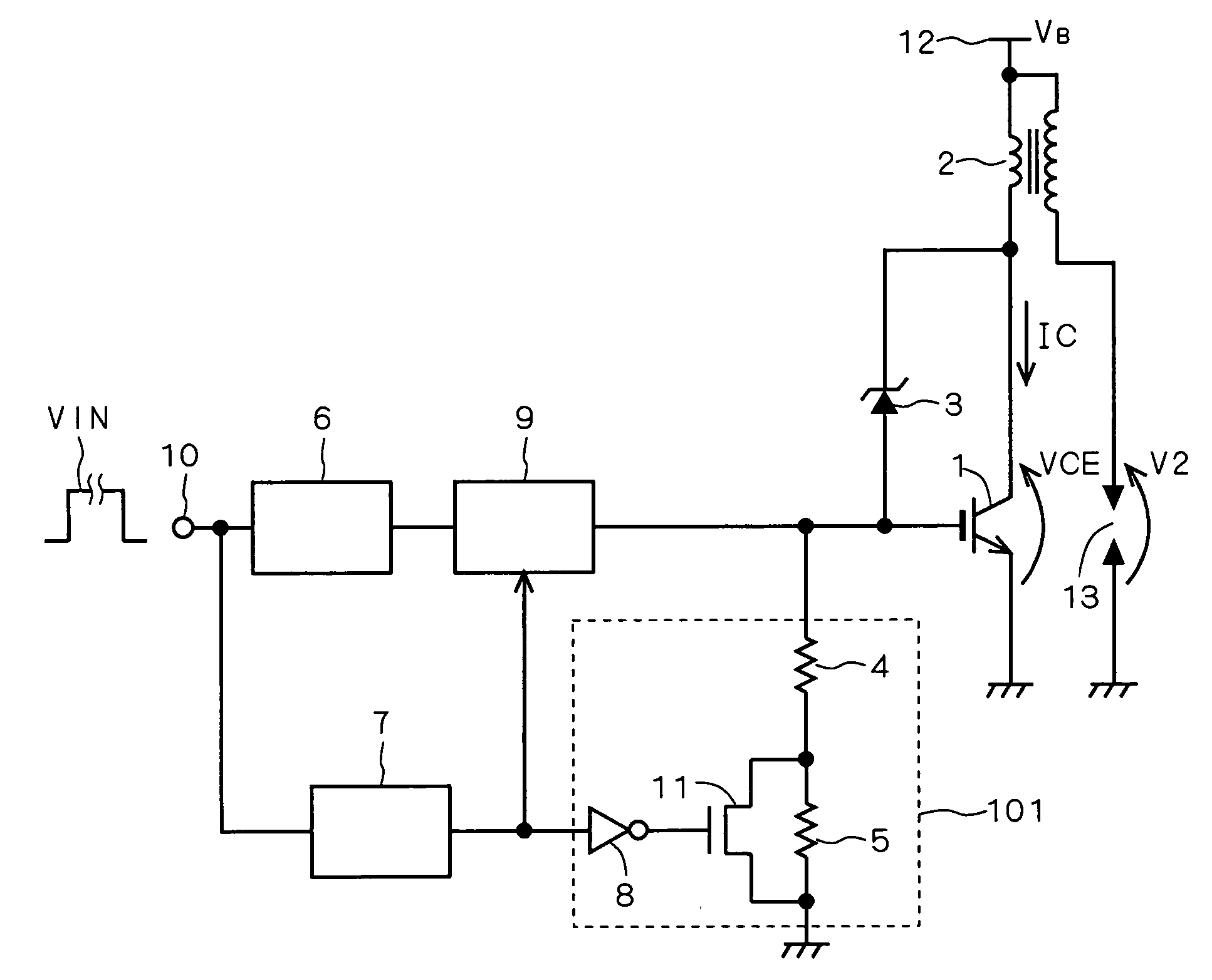
[0034]FIG. 1 is a circuit diagram showing a configuration of a semiconductor device according to the present embodiment. A control circuit 6 has its input connected to an input terminal 10 and its output connected to the input of a gate driving circuit 9. The gate driving circuit 9 has its output connected to the gate (control terminal) of an IGBT (Insulated Gate Bipolar Transistor) 1 serving as a switching device.

[0035] Upon receipt of an input signal VIN through the input terminal 10, the control circuit 6 controls the input signal VIN in response to a signal sent from a monitoring circuit (not shown) for monitoring the driving status of the IGBT 1, to output a control signal to the gate driving circuit 9. The gate driving circuit 9 drives the gate of the IGBT 1 in response to the control signal.

[0036] The IGBT 1 has its collector (current input terminal) connected to one end of a primary coil constituting a load coil (inductive load) 2 and the cathode of a Zener diode (clamping...

second preferred embodiment

[0072]FIG. 7 is a circuit diagram showing a configuration of a semiconductor device according to the present embodiment. A Zener diode 28 (second clamping device) has its cathode connected to the collector of the IGBT 1 and its anode connected to the source of a PMOS transistor 27 and one end of a resistor 29. The PMOS transistor 27 has its drain connected to the gate of the IGBT 1. A breakdown voltage in the Zener diode 28 is set at the same value as the Zener diode 3.

[0073] The resistor 29 has the other end connected to the gate of the PMOS transistor 27 and the drain of an NMOS transistor 26. The source of the NMOS transistor 26 is grounded. A buffer circuit 25 has its output connected to the gate of the NMOS transistor 26 and its input connected to the output of the timer circuit 7.

[0074] Since other configuration is the same as that described in the first preferred embodiment, similar components are indicated by the same reference numbers, and repeated explanation is omitted ...

third preferred embodiment

[0082]FIG. 8 is a circuit diagram showing a configuration of a semiconductor device according to the present embodiment. In the present embodiment, the resistor (discharge resistor part) 16 is connected to the gate of the IGBT 1 in place of the gate discharge resistor part 101. The Zener diode 28 is configured to have a breakdown voltage equal to a desired clamping voltage (e.g., approximately 30V) for clamping the voltage VCE.

[0083] Since other configuration is the same as that described in the second preferred embodiment, similar components are indicated by the same reference numbers, and repeated explanation is omitted here.

[0084] The operation of the semiconductor device according to the present embodiment will be described now. In the normal operation, an L-level signal output from the timer circuit 7 is input to the gate of the NMOS transistor 26 through the buffer circuit 25. The NMOS transistor 26 is brought into the OFF state, and the gate of the PMOS transistor 27 is not...


PUM


Abstract

A gate discharge resistor part is connected to the gate of an IGBT (Insulated Gate Bipolar Transistor). A timer circuit has its output connected to the input of the gate discharge resistor part and the input of a gate driving circuit. When an ON signal for driving the IGBT into an ON state stays input over a predetermined time period, the timer circuit outputs an H-level signal to the gate discharge resistor part and gate driving circuit. The gate driving circuit drives the IGBT into the OFF state based on the signal from the timer circuit. The gate discharge resistor part changes its resistance from a value given by a first resistor to a value given by a composite resistance of the first and second resistors.

Description

BACKGROUND OF THE INVENTION [0001] 1. Field of the Invention [0002] The present invention relates to a semiconductor device, and more particularly, to a technique of controlling overvoltage generated in an inductive load when forcedly stopping a switching device especially for the sake of protecting the semiconductor device. [0003] 2. Description of the Background Art [0004] An ignition system for an internal combustion engine such as an automobile engine has a problem in that a control signal is held “on” due to a misoperation or the like during maintenance, causing a switching device for controlling current in an inductive load (e.g., transformer or load coil) to be kept conducting, which results in degradation in characteristics or breakdown of a semiconductor device itself or load due to heat generation. [0005] Provided to solve this problem is a function of forcedly stopping a switching device using a timer circuit which operates after a lapse of a predetermined time period (ap...

Claims


Application Information

Patent Timeline
Patent Type & Authority Applications(United States)
IPC IPC(8): H03K17/687
CPCH03K17/08122H03K17/0822F02P3/051F02P9/002H03K17/08
Inventor GOUDO, SHINSUKE
Owner MITSUBISHI ELECTRIC CORP
Why Eureka
Try Eureka