

Method for applying metal features onto metallized layers using electrochemical deposition using acid treatment
- Summary
- Abstract
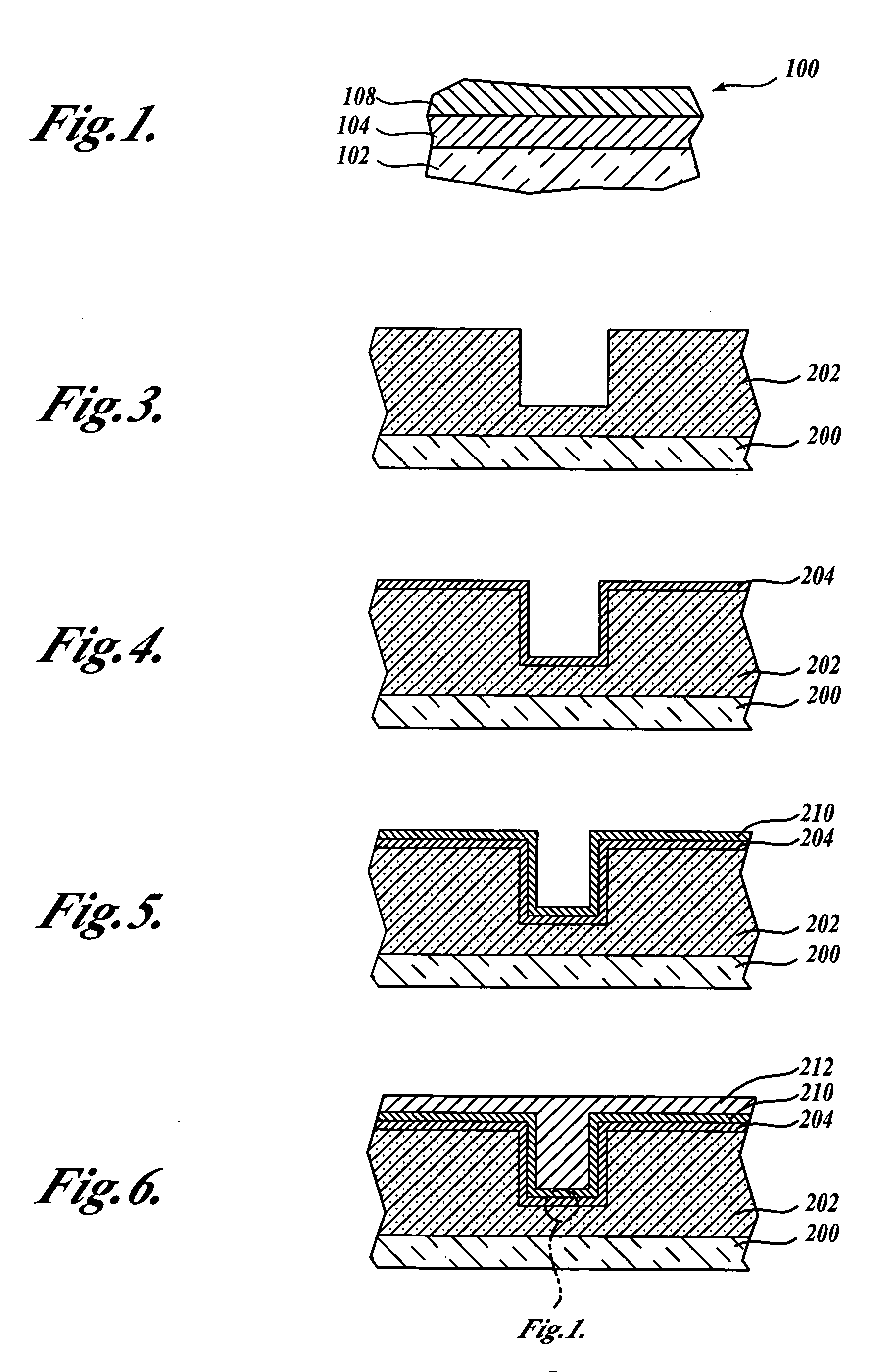
- Description
- Claims
- Application Information
AI Technical Summary
Benefits of technology
Problems solved by technology
Method used
Image

Examples
example 1
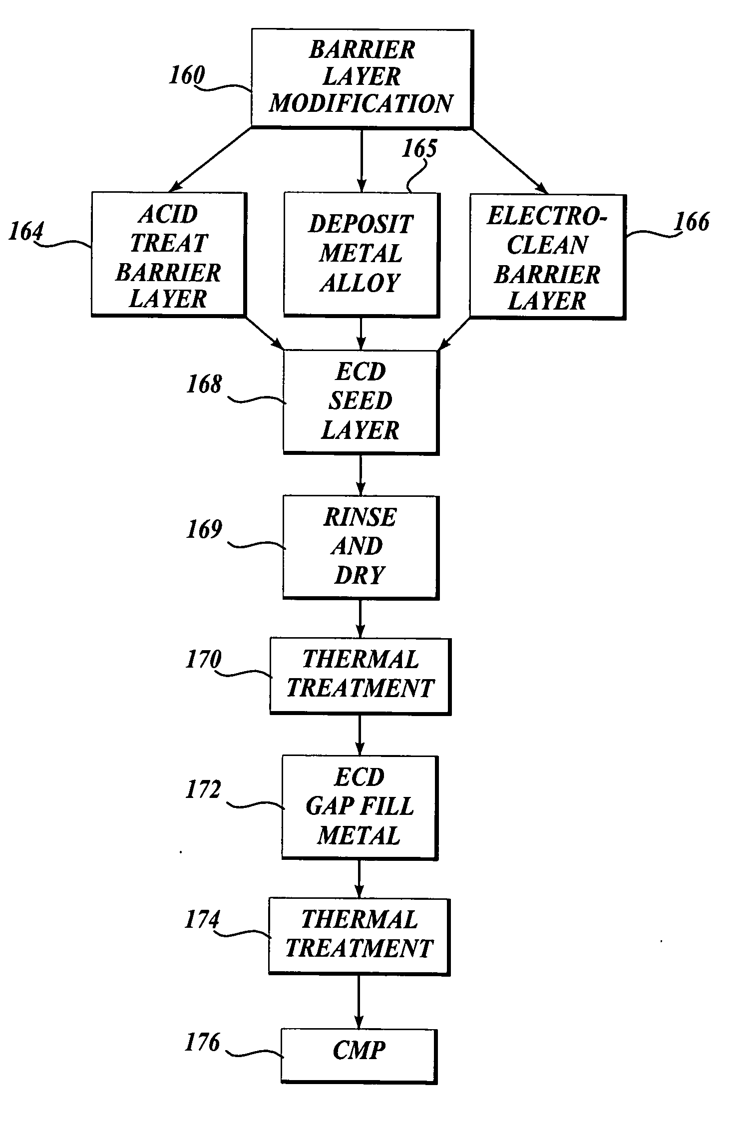
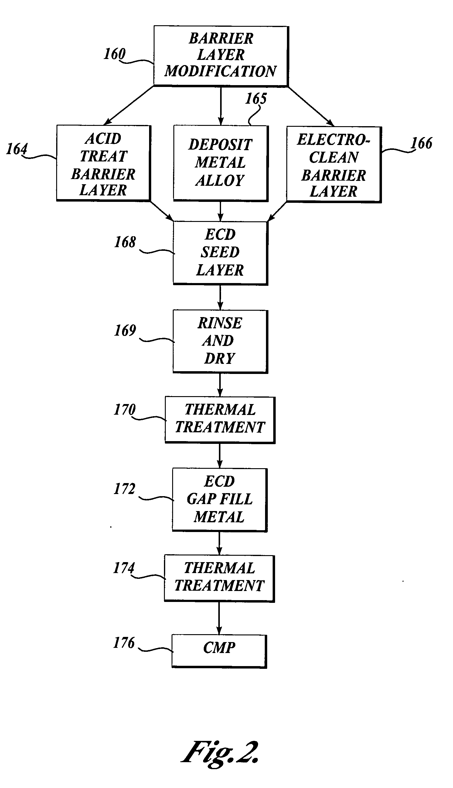
Acid Treatment of Barrier Layer
[0096] Acid treatment of a tantalum barrier was performed using 2% by weight aqueous solution of hydrofluoric acid. A 200 mm blanket wafer deposited with 25 nanometers of PVD tantalum barrier was used. This rotating wafer was subjected to a water spray treatment for 15 seconds followed by an acid spray treatment for 15 seconds. Then the rotating wafer was cleaned by spraying de-ionized water for another 15 seconds to remove the excess acid from its surface. For an additional 5 seconds, the wafer was rotated to sling off large water droplets. The wafer was then wet-transferred to a plating chamber. In the plating chamber, the wafer was plated with copper up to a thickness of ˜80 nanometers. After plating, the wafer was cleaned insitu with de-ionized water and the wafer was transferred to a SRD (Spin, Rinse, and Dry) chamber. In this SRD chamber, the spinning wafer was once again cleaned with de-ionized water thoroughly to remove any plating chemistry l...
example 2
Electrolytic Treatment of Barrier Layer
[0097] Electrolytic treatment of a tantalum barrier was performed using 2% by weight of potassium hydroxide aqueous solution. A 200 mm blanket wafer with 25 nanometers of PVD tantalum barrier was treated. This rotating wafer was used as a cathode and subjected to a current of 1 A (˜3 mA / cm2) for one minute while an inert platinum electrode was the anode. The wafer was then wet-transferred to a SRD chamber where the spinning wafer was rinsed with de-ionized water and then once again wet transferred to a plating chamber. In the plating chamber, the wafer was plated with copper up to a thickness of about 80 nanometers. After plating, the wafer was cleaned insitu with de-ionized water and the wafer was transferred to a SRD chamber. In this SRD chamber, the spinning wafer was once again cleaned with de-ionized water thoroughly to remove any plating chemistry left on its surface. After rinsing, the wafer was dried by spinning it in the chamber for s...
PUM
| Property | Measurement | Unit |
|---|---|---|
| Current density | aaaaa | aaaaa |
| Power | aaaaa | aaaaa |
Abstract
Description
Claims
Application Information