Using hole-or electron-blocking layers in color oleds
a color oled, electron block technology, applied in the manufacture of electrode systems, cold cathode manufacturing, electric discharge tube/lamp manufacture, etc., can solve the problems of adding to the time and complexity of manufacture, and achieve the effect of reducing the number of alignment and patterned transfer steps, reducing the number of handling steps, and simplifying the manufacturing process of color oled devices
- Summary
- Abstract
- Description
- Claims
- Application Information
AI Technical Summary
Benefits of technology
Problems solved by technology
Method used
Image
Examples
example 1
Inventive Example
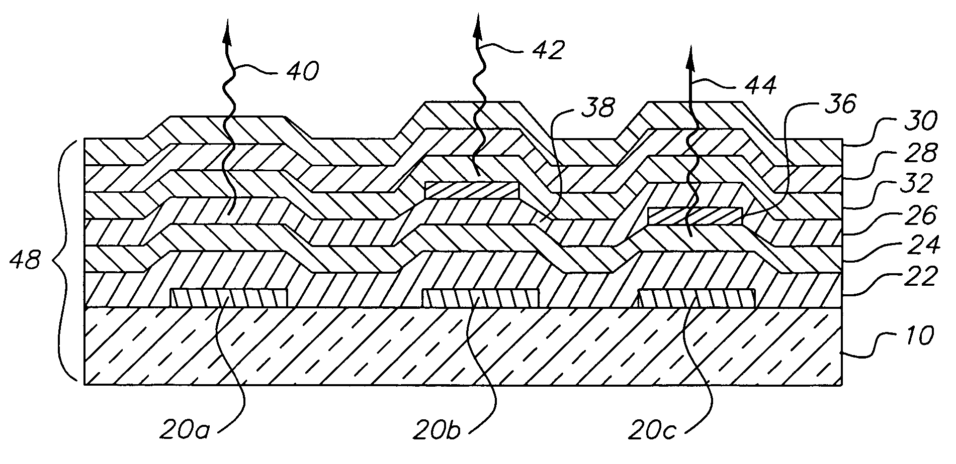
[0140] An OLED device with an electron-blocking layer satisfying the requirements of the invention was constructed in the following manner. [0141] 1. A clean glass substrate was vacuum-deposited with indium tin oxide (ITO) through a mask to form a pattern of transparent electrodes of 40 to 80 nm thickness. [0142] 2. The above-prepared ITO surface was treated with a plasma oxygen etch, followed by plasma deposition of a 0.1 nm layer of a fluorocarbon polymer (CFx) as described in U.S. Pat. No. 6,208,075. [0143] 3. The above-prepared substrate was further treated by vacuum-depositing a 40 nm layer of 4,4′-bis[N-(1-naphthyl)-N-phenylamino]biphenyl (NPB) as a hole-transporting layer followed by a 15.3 nm layer of of 2-tert-butyl-9,10-bis(2-naphthyl)anthracene (TBADN) with 2% 4-(dicyanomethylene)-2-t-butyl-6-(1,1,7,7-tetramethyljulolidyl-9-enyl)-4H-pyran (DCJTB) (a red dopant). [0144] 4. A coating of 30 nm of 1,1-bis(4-di-p-tolylaminophenyl)cyclohexane (TAPC) as the ele...
example 2
Comparative Example
[0149] An OLED device was constructed in the manner described in Example 1, except that Step 4 (the deposition of an electron blocker) was skipped.
example 3
Inventive Example
[0150] An OLED device with an electron-blocking layer satisfying the requirements of the invention was constructed in the manner described in Example 1, except Step 3 was performed as follows: [0151] 3. The above-prepared substrate was further treated by vacuum-depositing a 40 nm layer of 4,4′-bis[N-(1-naphthyl)-N-phenylamino]biphenyl (NPB) as a hole-transport layer followed by a 20.4 nm layer of of ALQ with 2% 4-(dicyanomethylene)-2-t-butyl-6-(1,1,7,7-tetramethyljulolidyl-9-enyl)-4H-pyran (DCJTB) (a red dopant).
PUM
 Abstract
Description
Claims
Application Information


