Electrostatic protective element of semiconductor integrated circuit
a technology of integrated circuits and protective elements, which is applied in the direction of semiconductor devices, semiconductor/solid-state device details, electrical apparatus, etc., can solve the problems of thermal runaway, breakdown, and low dc withstand voltage bvceo (=vh), so as to improve the uniformity of the action of transistors, reduce the start voltage vt1, and reduce the dispersion of esd breakdown resistance.
- Summary
- Abstract
- Description
- Claims
- Application Information
AI Technical Summary
Benefits of technology
Problems solved by technology
Method used
Image

Examples
first embodiment
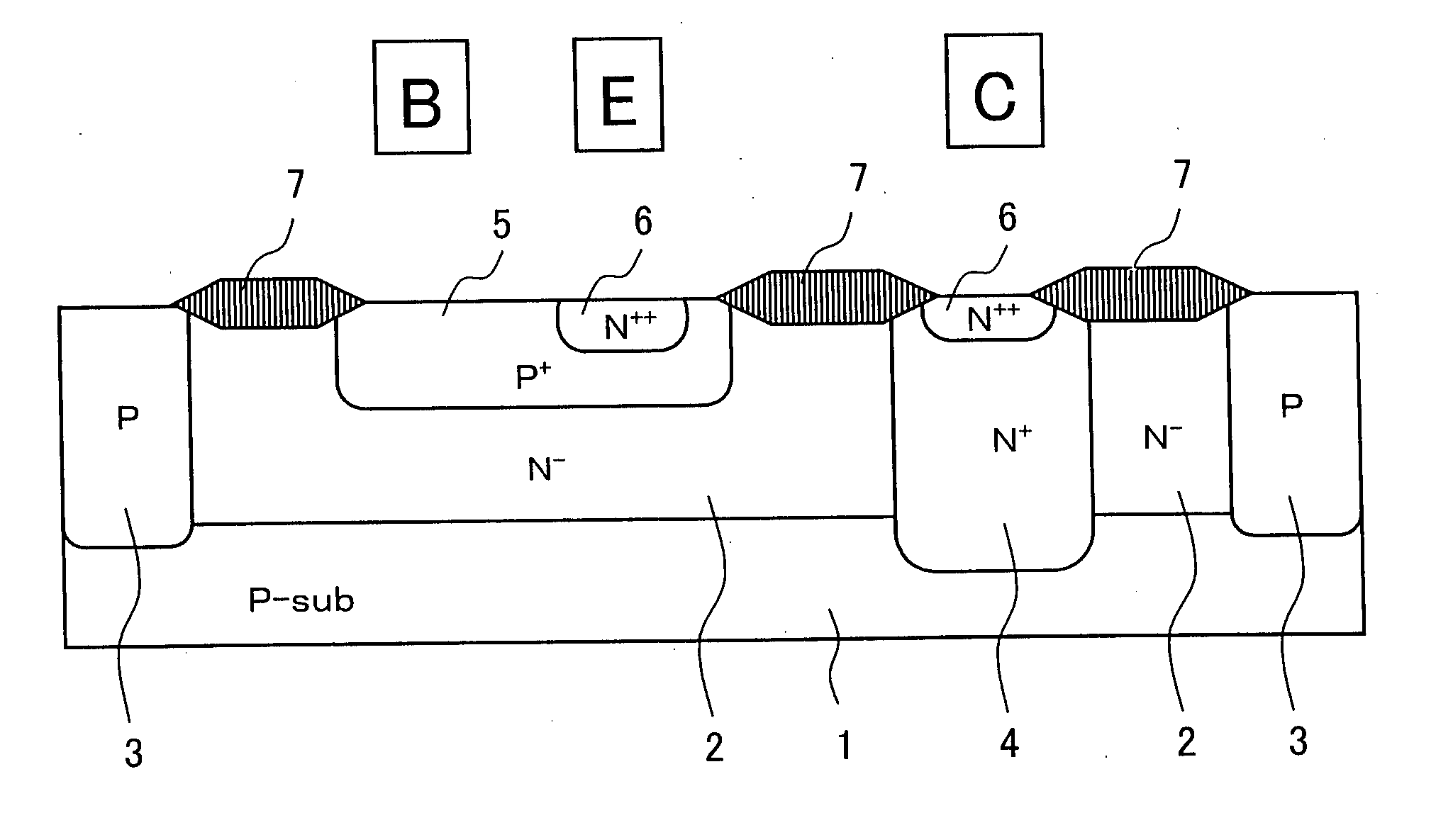
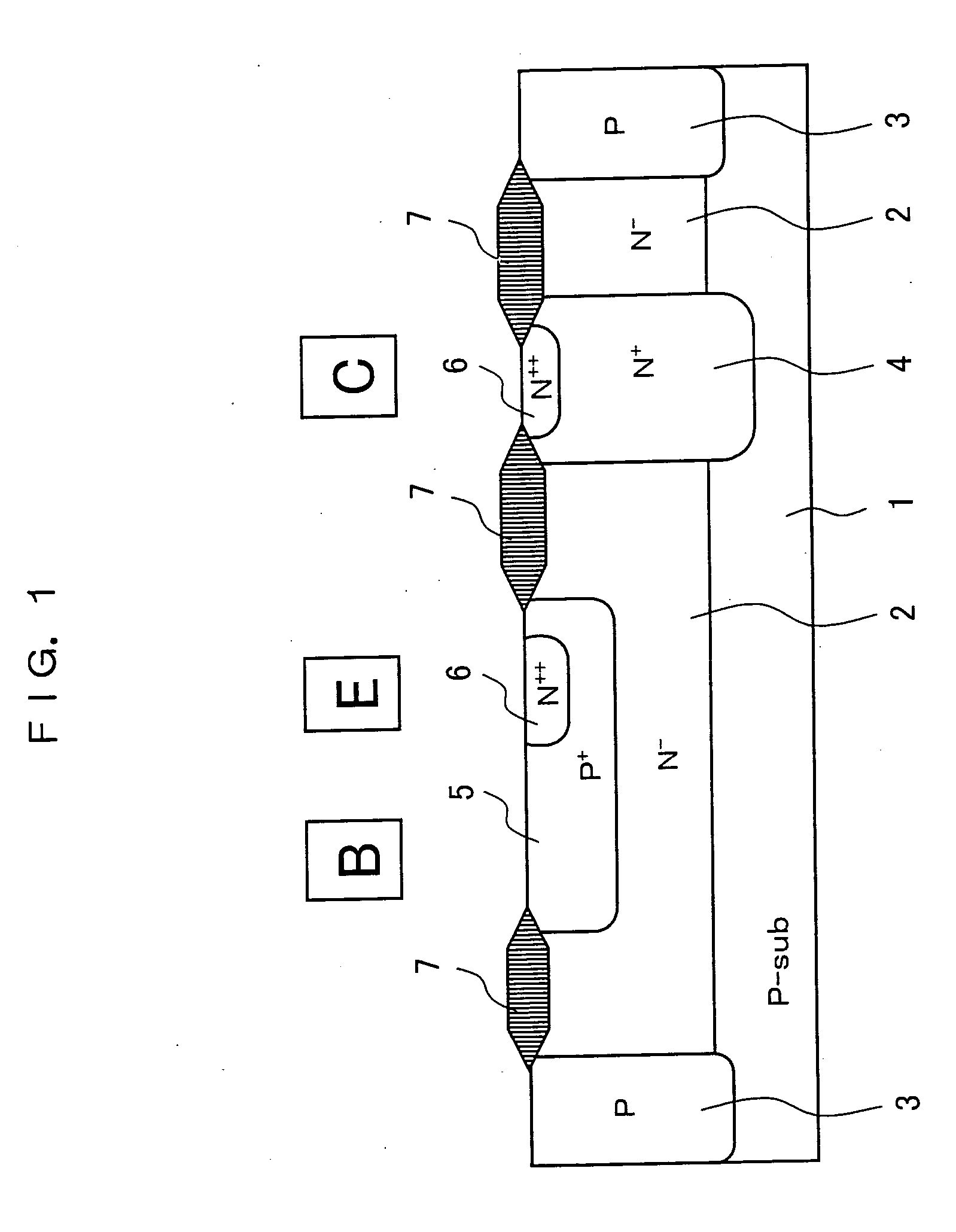
[0039] As shown in FIG. 1, the electrostatic protective element according to a first embodiment of the present invention has such a structure in which, in an NPN transistor which is formed with an N-type lightly-doped (N−) diffusion layer 2 serving as a collector layer being formed within a P-type substrate (silicon) 1, a P-type (P+) diffusion layer 5 serving as a base layer, and an N-type diffusion layer 6 serving as an emitter layer, a heavily-doped N-type diffusion layer 4 is formed in a contact area right under a collector electrode. Since the NPN transistor is in a structure with no embedded diffusion layer, the bottom face of the lightly-doped N-type diffusion layer 2 comes directly in contact with the P-type substrate 1 thereby forming pn junction between the collector and the substrate. The diffusion structure of the NPN transistor used in an internal circuit is not formed to have the heavily-doped N-type diffusion layer 4. Reference numeral 3 is an element isolation layer a...
second embodiment
[0048] Next, an electrostatic protective element of a semiconductor integrated circuit according to a second embodiment of the present invention will be described. This is aimed for improving the non-uniform actions.
[0049] As shown in FIG. 5 and FIG. 6, an anode A of a diode 9 is connected to a base B of an electrostatic protective element 8, a cathode K of the diode 9 is connected to a collector C, and the base B is connected to an emitter E through a resistance 10. Further, the base B is connected to an input / output terminal 11 through the diode 9, the collector C is connected to the input / output terminal 11, and the emitter E is connected to a minimum potential terminal 12.
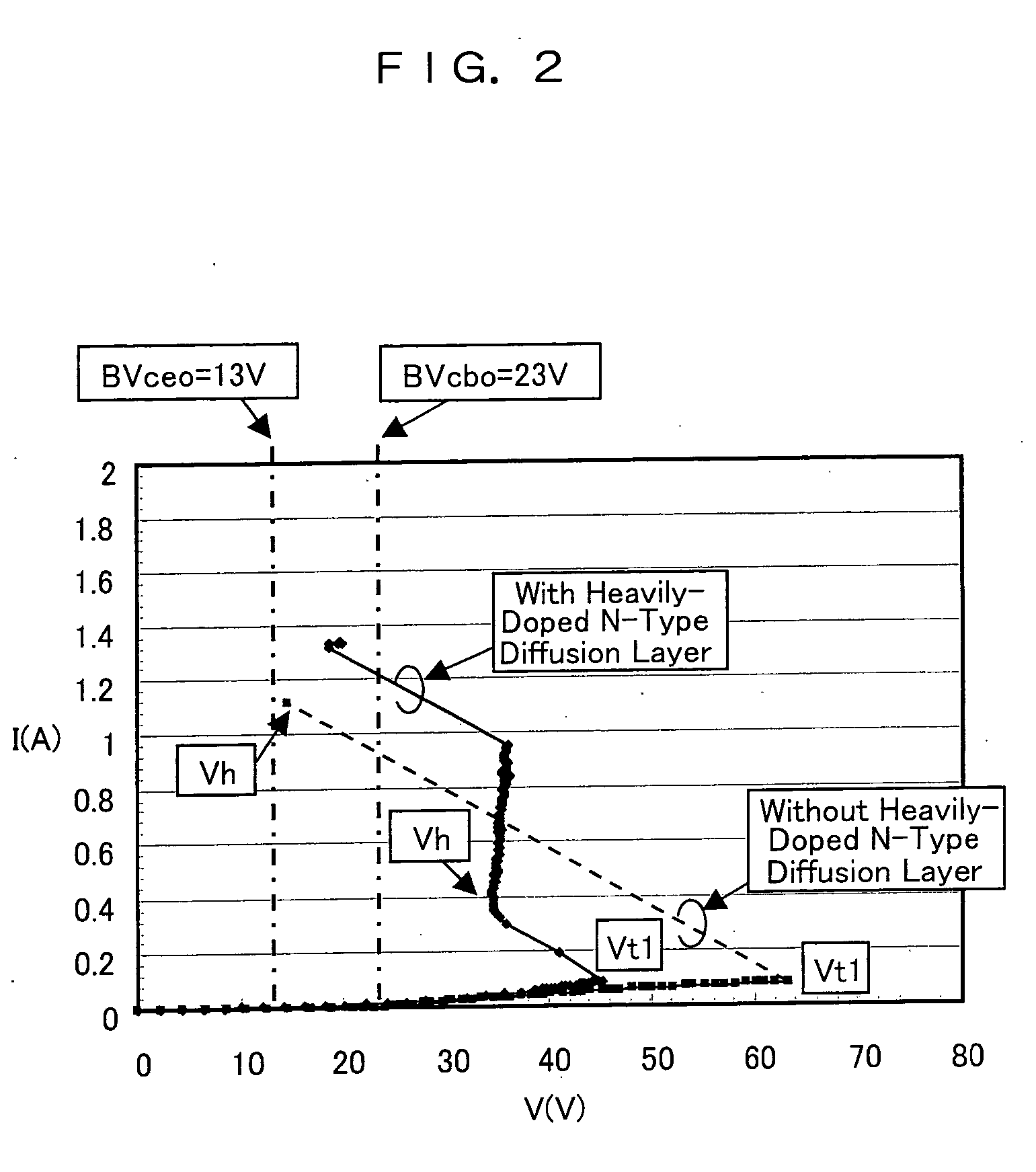
[0050] In general, when the ESD breakdown voltage Vt2 of the NPN transistor is lower than the snapback action start voltage Vt1, breakdown is caused at a voltage lower than the actual withstand voltage. Meanwhile, when the ESD braking voltage Vt2 is higher than the snapback action start voltage Vt1, breakdown...
PUM
 Abstract
Description
Claims
Application Information
 - R&D
- Intellectual Property
- Life Sciences
- Materials
- Tech Scout
- Unparalleled Data Quality
- Higher Quality Content
- 60% Fewer Hallucinations
Browse by: Latest US Patents, China's latest patents, Technical Efficacy Thesaurus, Application Domain, Technology Topic, Popular Technical Reports.
© 2025 PatSnap. All rights reserved.Legal|Privacy policy|Modern Slavery Act Transparency Statement|Sitemap|About US| Contact US: help@patsnap.com