Method for manufacturing electronic device

a manufacturing method and electronic device technology, applied in semiconductor/solid-state device manufacturing, basic electric elements, electric devices, etc., can solve problems such as generating transmission delays, reducing signal propagation rates, and increasing problems, so as to improve the production yield of electronic devices, improve quality, and improve controllability

Inactive Publication Date: 2006-05-04
NEC ELECTRONICS CORP
View PDF5 Cites 27 Cited by
  • Summary
  • Abstract
  • Description
  • Claims
  • Application Information

AI Technical Summary

Benefits of technology

[0013] Such configuration according to the present invention provides an inhibition to the resist poisoning in the formation of the resist mask having the interconnect-patterned trench opening, and also provides a formation of the trench for dual damascene interconnect having fine structure and better quality and the dual damascene interconnect formed by plugging thereof with an interconnect material film under higher controllability, thereby considerably improving a production yield of the electronic device comprising the dual damascene interconnects.
[0014] According to the configuration of the present invention, the resist poisoning can be inhibited in the formation of the resist mask having certain openings to provide a production of the electronic device having fine structure and better quality.

Problems solved by technology

In recent years, remarkably increasing processing speed of the semiconductor device leads to a problem of generating a transmission delay due to a decrease in a signal propagation rate, which is caused by an interconnect resistance in a multi-layer interconnect and a parasitic capacitance between the interconnects.
Such problem tends to become more and more considerable, due to an increased interconnect resistance and an increased parasitic capacitance, which are caused in accordance with miniaturizations of a line width and an interconnect interval created by an increased integration of the semiconductor device.
However, the formation process for the dual damascene interconnect employing the above-described via first method may cause a problem, in which so-called resist poisoning phenomenon is typically generated on the resist mask that is employed for forming the trenches for interconnects.
Therefore, a problem of difficulties in forming the trench openings of the resist mask with higher minuteness and precision is arisen.

Method used


Image

  • Method for manufacturing electronic device
  • Method for manufacturing electronic device
  • Method for manufacturing electronic device

Examples


Embodiment Construction

[0025] The invention will be now described herein with reference to illustrative embodiments. Those skilled in the art will recognize that many alternative embodiments can be accomplished using the teachings of the present invention and that the invention is not limited to the embodiments illustrated for explanatory purposed.

[0026] Preferred embodiments of the present invention will be described as follows in reference to the annexed figures.

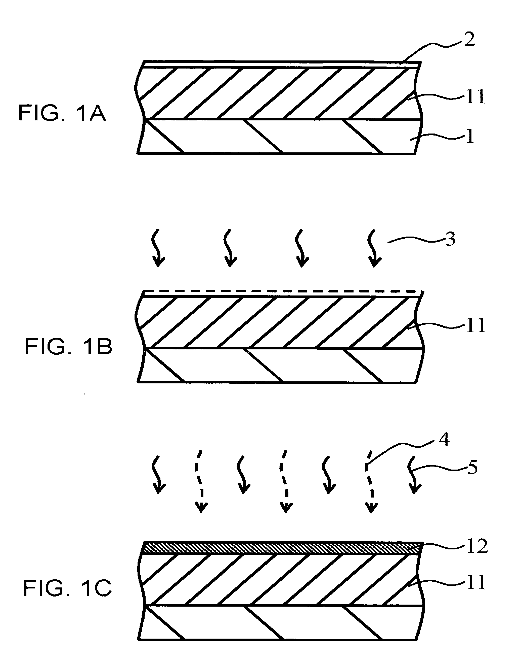
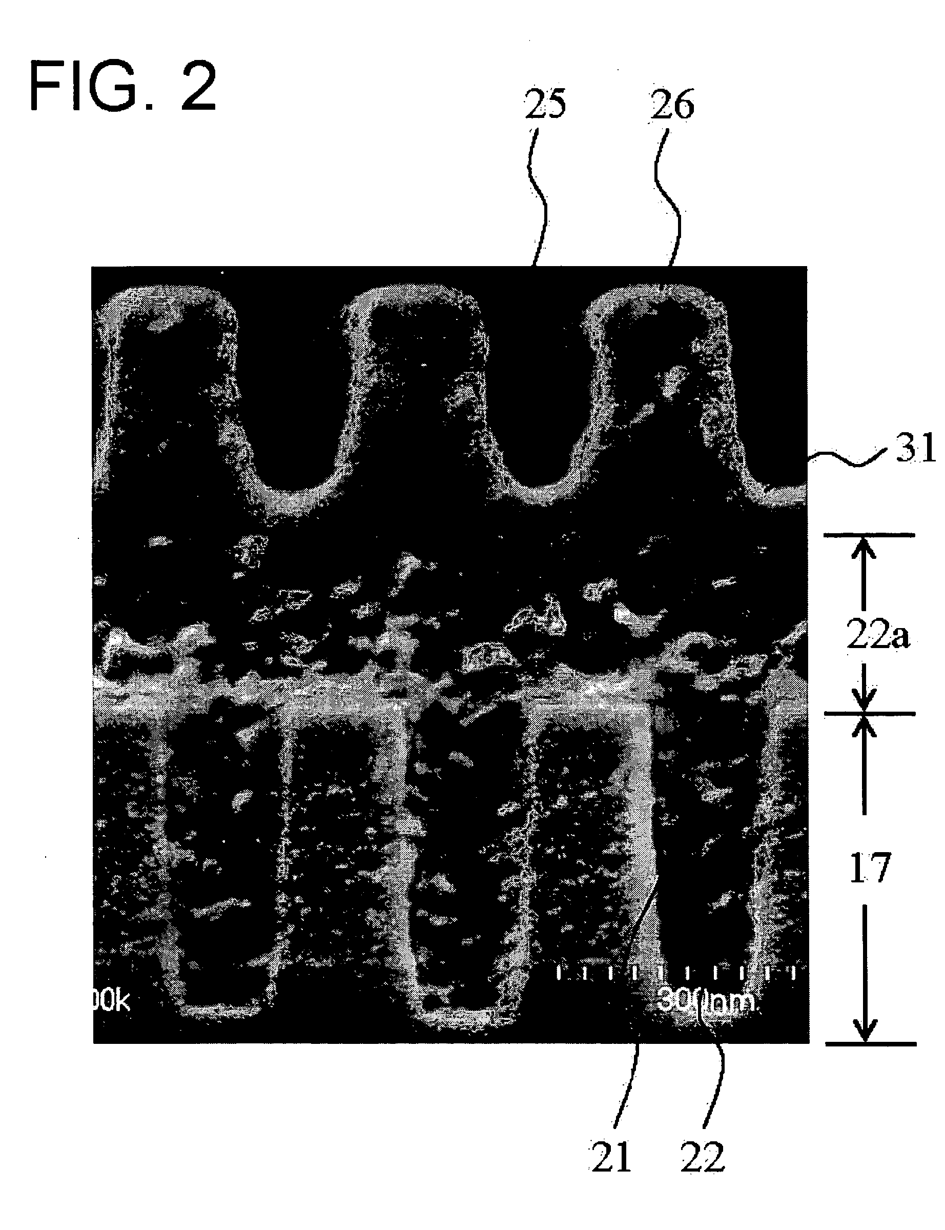
[0027] The present inventor had studied the resist poisoning phenomenon. The phenomenon will be described as follows in reference to FIGS. 9A and 9B.

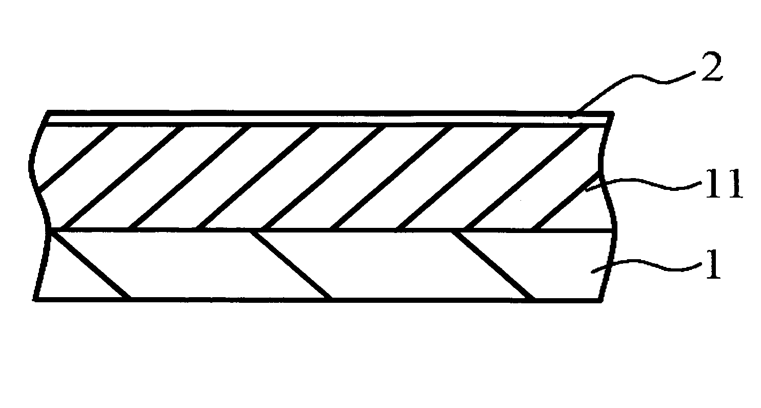
[0028] When a photo resist for ArF excimer laser exposure, for example, is irradiated with light and then developed, in order to form the second resist mask 26 using a chemically amplified positive resist in the photolithography process, the resist in the region around the trench opening 25 is not fully dissolved, resulting in a developing failure and a generation of a remaining resist (scum) 31 ...


PUM

PropertyMeasurementUnit
relative dielectric constantaaaaaaaaaa
dielectric constantaaaaaaaaaa

Abstract

The method for manufacturing an electronic device is provided. The method includes: applying an active hydrogen species over a surface of an underlying interconnect formed on a substrate and having an anti-corrosion material formed on the surface thereof and containing copper, to remove the anti-corrosion material; and forming an insulating barrier layer, which functions as a copper diffusion barrier film, on the underlying interconnect via a chemical vapor deposition or an atomic layer deposition employing a reactive gas of a mixture of an organosilane gas and an active nitrogen species. The active hydrogen species is generated from hydrogen gas or a gaseous mixture of hydrogen gas and inert gas, and the active nitrogen species is generated from nitrogen gas or a gaseous mixture of nitrogen gas and inert gas, and the active hydrogen species and the active nitrogen species are separately generated and used, respectively.

Description

[0001] This application is based on Japanese Patent Application NO. 2004-317,718, the content of which is incorporated hereinto by reference. BACKGROUND [0002] 1. Technical Field [0003] The present invention relates to a method for manufacturing an electronic device. [0004] 2. Related Art [0005] In recent years, remarkably increasing processing speed of the semiconductor device leads to a problem of generating a transmission delay due to a decrease in a signal propagation rate, which is caused by an interconnect resistance in a multi-layer interconnect and a parasitic capacitance between the interconnects. Such problem tends to become more and more considerable, due to an increased interconnect resistance and an increased parasitic capacitance, which are caused in accordance with miniaturizations of a line width and an interconnect interval created by an increased integration of the semiconductor device. Consequently, in order to prevent a signal delay caused on the basis of enhance...

Claims


Application Information

Patent Timeline
Patent Type & Authority Applications(United States)
IPC IPC(8): H01L21/44
CPCH01L21/02074H01L21/31116H01L21/31138H01L21/31144H01L21/3148H01L21/318H01L21/321H01L21/76808H01L21/76838H01L21/0228H01L21/02271
Inventor SODA, EIICHI
Owner NEC ELECTRONICS CORP
Why Eureka
Try Eureka