Method and apparatus for leveling a semiconductor wafer, and semiconductor wafer with improved flatness

a technology of semiconductor wafers and flatness, which is applied in the direction of semiconductor devices, solid-state devices, testing/measurement of semiconductor/solid-state devices, etc., can solve the problems of complex process in terms of equipment required, disruptive edge roll off, and inability to ensure the flatness required for the ever-decreasing line. , to achieve the effect of improving nanotopography, improving the uniformity of layer thicknesses, and improving flatness

Inactive Publication Date: 2006-05-11
SILTRONIC AG
View PDF13 Cites 46 Cited by
  • Summary
  • Abstract
  • Description
  • Claims
  • Application Information

AI Technical Summary

Benefits of technology

[0020] An object of the invention is to provide a semiconductor wafer with improved flatness, in particular in the edge region, and improved nanotopography, which is suitable for the production of components with line widths of 65 nm or less. In this context, the term “semiconductor wafer” also encompasses an SOI wafer. A further object is to provide an SOI wafer with improved layer thickness homogeneity, in particular in the edge region.

Problems solved by technology

An edge roll off is disruptive in particular in the case of semiconductor wafers which, for example to produce SOI wafers, are bonded to a further semiconductor wafer, since the edge roll off of the wafer surfaces which are to be bonded to one another has a considerable influence on the bonding quality at the edge of the wafer.
It has been found that this process sequence is unable to ensure the flatnesses required for the ever-decreasing line widths.
Furthermore, it does not state the size of the edge exclusion for the flatness measurement.
PACE has to be carried out in vacuo, which makes the process complex in terms of the equipment required.
This is, on the one hand, very time-consuming, and on the other hand, leads to problems with regard to the nanotopography in the scanning overlap region and to problems with regard to flatness (SFQRmax and edge roll off) in the outer region of the semiconductor wafer, up to a distance of approx.
The required overlap during scanning has an adverse effect in particular on the nanotopography at the overlap positions.
The larger the diameter of the nozzle which is used to supply the etching medium, the worse the deterioration becomes.
However, for economic reasons the nozzle diameter cannot be selected to be as small as may be desirable.
Consequently, the methods which are known in the prior art are unable to satisfy the geometry requirements for components with line widths of less than or equal to 65 nm, that is to say SFQRmax values of at most 65 nm.
An additional problem arises in the case of what are known as SOI wafers.
This chemical mechanical polishing step on the one hand reduces the roughness, but on the other hand also has a significant adverse effect on the layer thickness homogeneity, in particular at the edge of the wafer.
All methods in which the surface of the semiconductor layer has to be scanned in order to achieve a locally different removal of material by etching are very time-consuming and therefore expensive.
Therefore, despite the complex methods, the required layer thickness homogeneities are not achieved, in particular in the edge region of the SOI wafer.

Method used


Image

  • Method and apparatus for leveling a semiconductor wafer, and semiconductor wafer with improved flatness
  • Method and apparatus for leveling a semiconductor wafer, and semiconductor wafer with improved flatness
  • Method and apparatus for leveling a semiconductor wafer, and semiconductor wafer with improved flatness

Examples


example 1

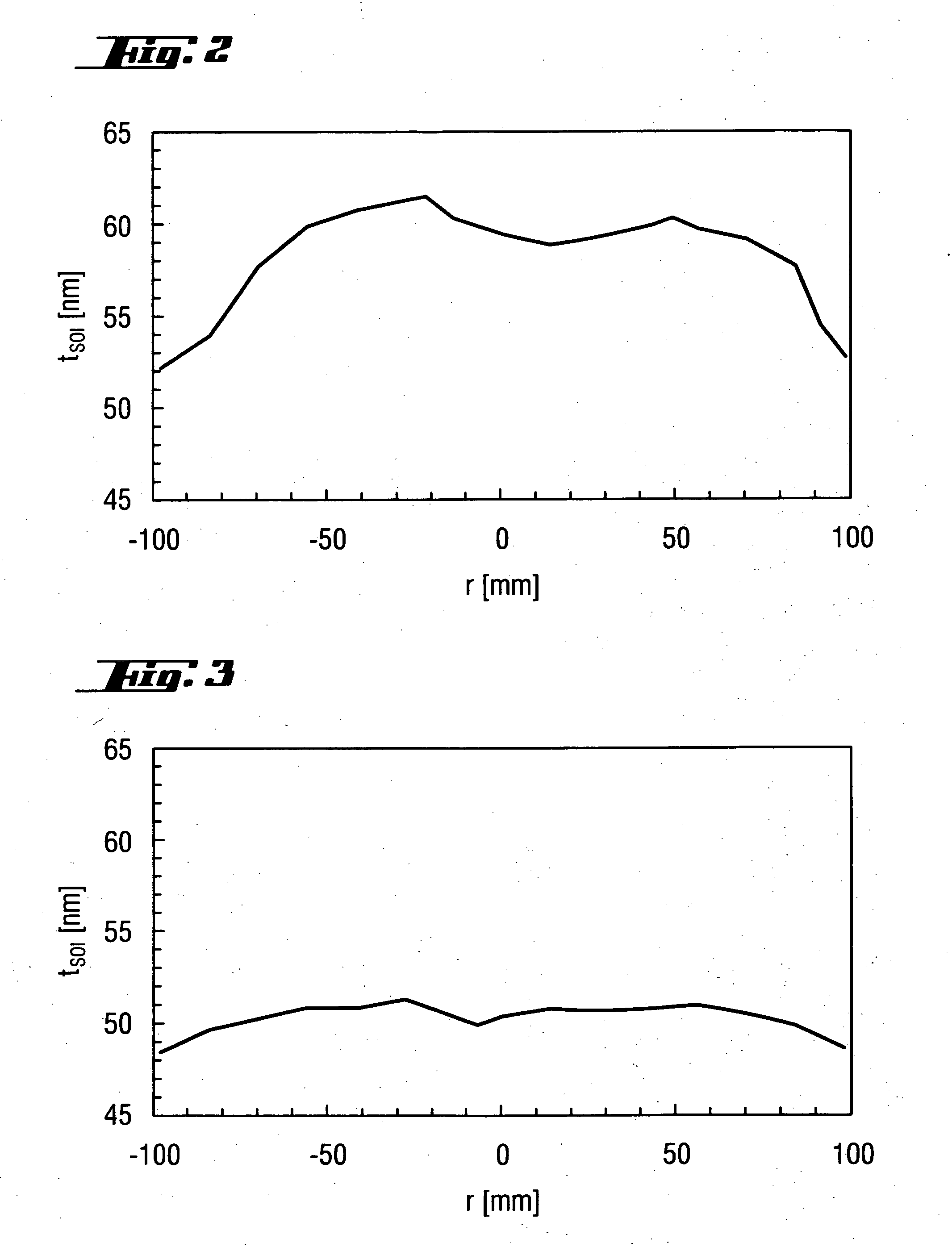
[0096] An SOI wafer with a diameter of 200 mm, produced by transferring a silicon layer from a donor wafer to a base wafer, is treated. The thickness of the wafer is 730 μm, the thickness of the silicon oxide layer is 140 μm, and the target thickness of the silicon layer located on the silicon oxide layer is 50 nm.

[0097] In step a), the thickness of the silicon layer is measured accurately in a position-dependent manner by means of an interferometer. The measurement with 4000 measurement points and an edge exclusion of 1 mm gives a mean layer thickness of 58.3 nm with a standard deviation of 2.9 nm and a difference of 9.4 nm between maximum and minimum layer thickness. FIG. 2 illustrates a thickness profile along a diameter, i.e. the thickness tSOI of the semiconductor layer, measured in the unit nm, as a function of the radial position r, measured in the unit mm. The thickness measured values are stored in a computer and converted into a grayscale contrast filter. Positions with a...

example 2

[0100] In step a), the local flatness of 6 silicon wafers with a diameter of 300 mm, which were produced from a Czochralski-pulled, boron-doped (1-10 Ωcm) single crystal, and had been subjected to stock-removal polishing, measured with an edge exclusion of 1 mm. The measuring unit ADE 9900 E+ is used, and the size of the surface elements is 26×8 mm2. Table 1 shows the measured SFQRmax values including partial sites.

[0101] The unprocessed data (individual measured values) from the ADE measurement are stored in a computer and converted into a grayscale contrast filter, and a corresponding filter is produced for each silicon wafer. Then, the silicon wafers are introduced into the etching chamber individually, as described in Example 1, and subjected to an etching treatment on one side for leveling purposes using the associated filter. The etching medium used is an aqueous solution of 1% HF and 20 ppm O3. The silicon wafers are treated for approximately 10 minutes at room temperature, ...


PUM

PropertyMeasurementUnit
sizeaaaaaaaaaa
sizeaaaaaaaaaa
sizeaaaaaaaaaa

Abstract

Semiconductor wafers are leveled by a) position-dependent measurement of a wafer-characterizing parameter to determine the position-dependent value of this parameter over an entire surface of the semiconductor wafer, b) etching the entire surface of the semiconductor wafer simultaneously under the action of an etching medium with simultaneous illumination of the entire surface, the material-removal etching rate dependent on the light intensity at the surface of the semiconductor wafer, the light intensity being established in a position-dependent manner such that the differences in the position-dependent values of the parameter measured in step a) are reduced by the position-dependent material-removal rate, semiconductor wafers with improved flatness and nanotopography and SOI wafer with improved layer thickness homogeneity are achieved. An apparatus for carrying out the method is also disclosed.

Description

BACKGROUND OF THE INVENTION [0001] 1. Field of the Invention [0002] The present invention relates to a method and an apparatus for leveling a semiconductor wafer by means of an etching treatment with locally different removal of material. The invention also relates to both a semiconductor wafer with improved flatness and nanotopography and to an SOI wafer with a homogenous layer thickness which are obtainable by the method. [0003] 2. Background Art [0004] A semiconductor wafer, in particular a single-crystal silicon wafer for use in the semiconductor industry, has to have a high flatness, in particular in order to meet the requirements for the production of integrated circuits. A generally recognized rule of thumb states that the SFQRmax value of a semiconductor wafer must be no greater than the line width of the components which are to be produced on the semiconductor wafer. To allow the integration of the maximum possible number of circuits, the required flatness must moreover ext...

Claims


Application Information

Patent Timeline
Patent Type & Authority Applications(United States)
IPC IPC(8): H01L29/06H01L21/461C23F1/00
CPCH01L21/02019H01L21/30604H01L21/3065H01L22/12H01L2924/0002H01L22/20H01L2924/00H01L27/13B82Y40/00
Inventor BAUER, THERESIAHOELZL, ROBERTHUBER, ANDREASWAHLICH, REINHOLD
Owner SILTRONIC AG
Why Eureka
Try Eureka