Vertical Hall device and method for adjusting offset voltage of vertical Hall device

a vertical hall and offset voltage technology, applied in the direction of galvano-magnetic devices, galvano-magnetic hall-effect devices, instruments, etc., can solve the problems of unbalanced potential distribution within the element, unbalanced resistance bridge as an equivalent circuit of a resistance component within the element, and room for improvement, so as to achieve easy and accurate determination

Inactive Publication Date: 2006-05-11
DENSO CORP
View PDF10 Cites 78 Cited by
  • Summary
  • Abstract
  • Description
  • Claims
  • Application Information

AI Technical Summary

Benefits of technology

[0060] In this case, without adding a temperature sensor, the offset voltage is e...

Problems solved by technology

However, the vertical Hall element is not always in a structure that can meet the temporal circumstance where the element is placed, or a structure that is optimized depending on use of the Hall element and use of a sensor using the element, or use environment, and there is room for improvement (., problems).
When such stress is applied to the substrate, uneven stress is applied to respective portions of the substrate, and a resistance bridge as an equivalent circuit of a resistance component within the element becomes more unbalanced due to the piezoresistance effect.
That is, again in this case, unbalance occurs in the potential distribution within the element, consequently offset voltage is generated.
Such variation in output voltage due to the offset voltage or the temperature characteristic hinders accurate magnetic field detection.
However, even in such a case, when the variation in output voltage (for example, standard deviation) is large, the correction circuit must be enlarged, and therefore various inconveniences along with it become inevitable.
While the expansion of the correction circuit causes the inconveniences in either case, particularly in the case that the correction circuit is integrated into one chip, many inconveniences such as spa...

Method used


Image

  • Vertical Hall device and method for adjusting offset voltage of vertical Hall device
  • Vertical Hall device and method for adjusting offset voltage of vertical Hall device
  • Vertical Hall device and method for adjusting offset voltage of vertical Hall device

Examples


first embodiment

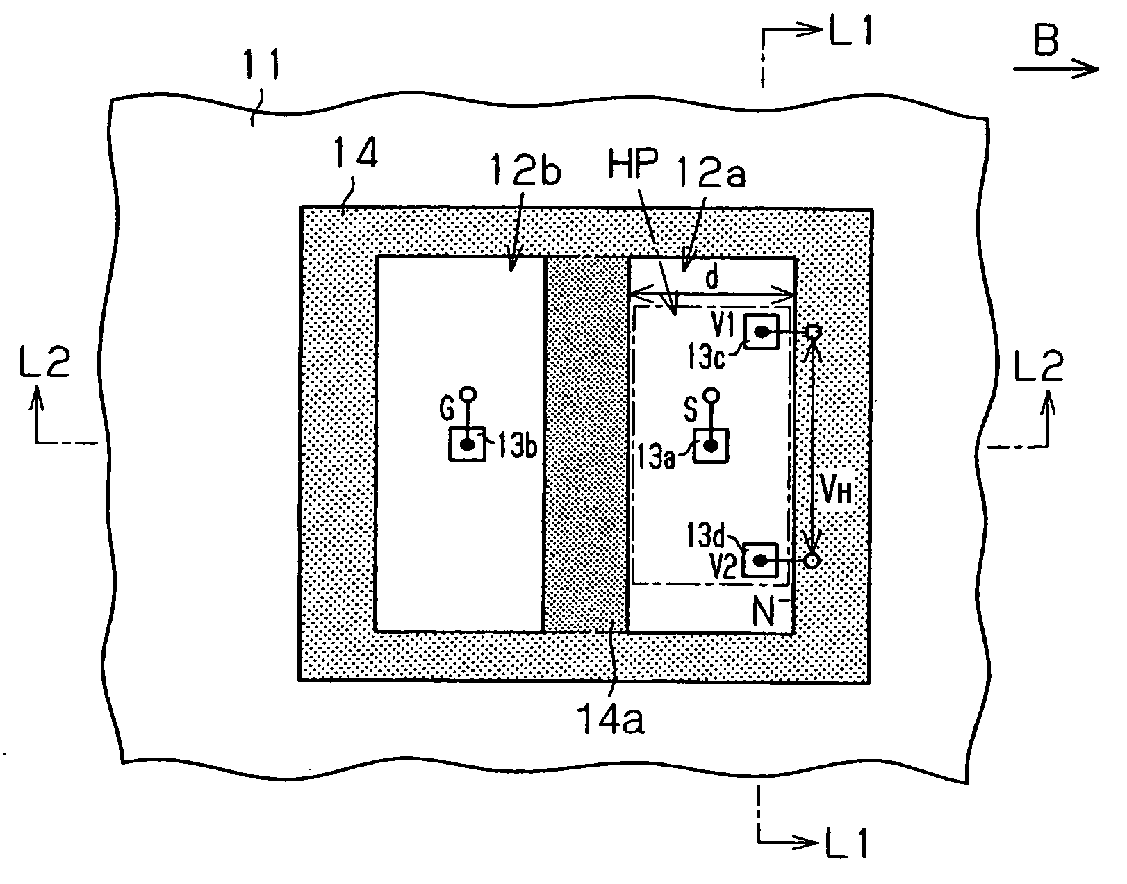
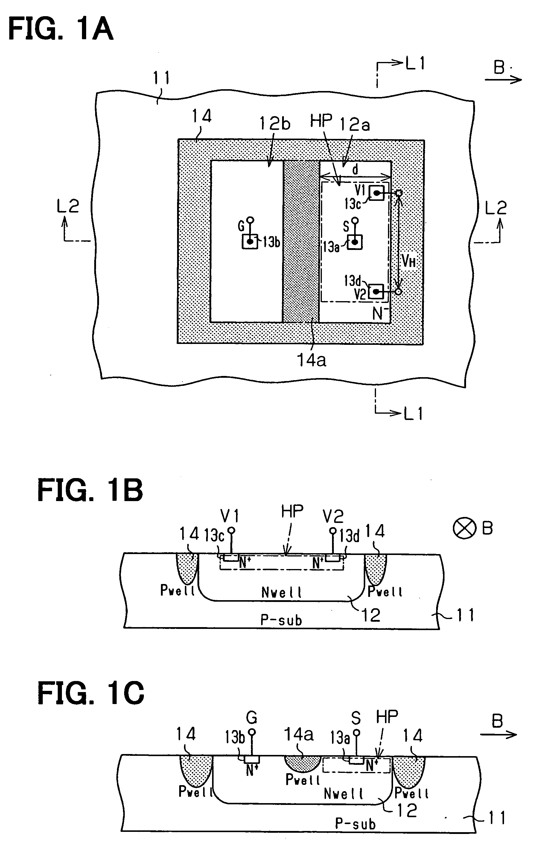
[0142] Hereinafter, a first embodiment of a vertical Hall element according to the invention is represented.

[0143] First, a schematic structure of the vertical Hall element according to the embodiment and an operation mode of the element are described with reference to FIG. 1A to FIG. 1C. In FIG. 1A to FIG. 1C, FIG. 1A is a plan view typically showing a planar structure of the Hall element, FIG. 1B is a cross section view along a line L1-L1 of FIG. 1A, and FIG. 1C is a cross section view along a line L2-L2 of FIG. 1A.

[0144] As shown in FIGS. 1A to 1C, the Hall element is roughly configured to have a semiconductor layer (i.e., P−sub) 11 comprising, for example, P-type silicon, and a N-type semiconductor region (i.e., N well) 12 formed as a diffusion layer (i.e., well), for example, by introducing an N-type conductivity type impurity into a surface of the layer 11. As described before, in the semiconductor material such as silicon, since N-type semiconductor has large carrier mobili...

second embodiment

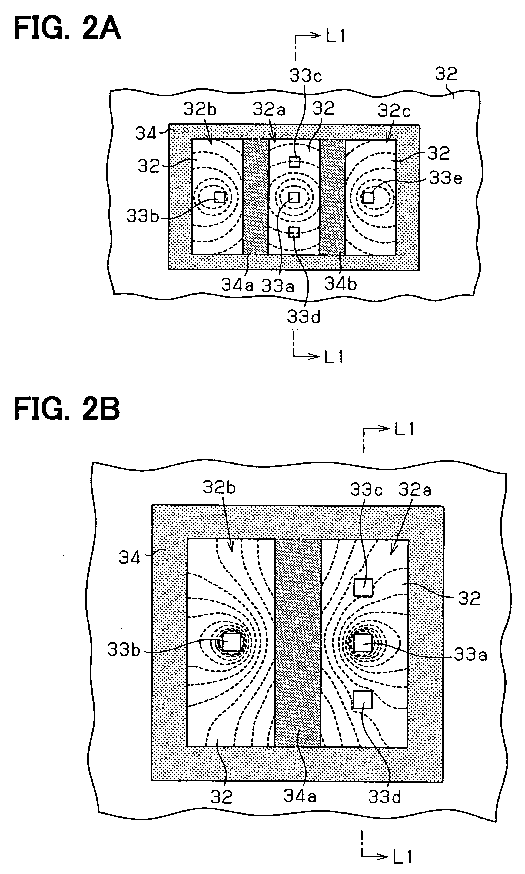
[0170]FIG. 7 shows a second embodiment of a vertical Hall element according to the invention.

[0171] Hereinafter, a structure of the vertical Hall element according to the embodiment is described with reference to FIG. 7 mainly on different points from the previous first embodiment. A plan view of the FIG. 7 corresponds to the plan view of the previous FIG. 1A, and respective elements identical to the elements shown in the FIG. 1A are shown with being marked with identical signs, and overlapped description on the elements is omitted.

[0172] As shown in the FIG. 7, the vertical Hall element has the approximately same structure as the vertical Hall element of the previous first embodiment exemplified in FIG. 1A to FIG. 1C, in addition, an operation mode of the element is the same as the mode described before. That is, in the vertical Hall element, a structure is made, wherein in the periphery of the axis (line L1-L1) given by the contact regions 13c and 13d provided as the portions fo...

third embodiment

[0175]FIG. 8 shows a third embodiment of a vertical Hall element according to the invention.

[0176] Hereinafter, a structure of the vertical Hall element according to the embodiment is described with reference to FIG. 8 mainly on different points from the previous first embodiment. A plan view of FIG. 8 corresponds to the plan view of the previous FIG. 1A, and respective elements identical to the elements shown in FIG. 1A are shown with being marked with identical signs, and overlapped description on the elements is omitted.

[0177] As shown in the FIG. 8, the vertical Hall element has the approximately same structure as the vertical Hall element of the previous first embodiment exemplified in FIG. 1A to FIG. 1C, and an operation mode of the element is also the same as the mode described before. However, in the embodiment, a structure is made, wherein the diffusion layer 14 provided for isolating the relevant Hall element from other elements is omitted. Thus, simplification of the st...


PUM


Abstract

A vertical Hall device includes: a semiconductor substrate including a magnetic field detection portion, a current portion and an output portion. The output portion includes a pair of output terminals. The current portion is capable of supplying the current to the magnetic field detection portion and retrieving the current from the magnetic field detection portion. The current portion is sandwiched between a pair of the output terminals in such a manner that the current portion is disposed apart from a line connecting between a pair of the output terminals.

Description

CROSS REFERENCE TO RELATED APPLICATIONS [0001] This application is based on Japanese Patent Applications No. 2004-314416 filed on Oct. 28, 2004, No. 2004-328907 filed on Nov. 12, 2004, No. 2004-333355 filed on Nov. 17, 2004, and No. 2005-110234 filed on Apr. 6, 2005, the disclosures of which are incorporated herein by reference. FIELD OF THE INVENTION [0002] The present invention relates to a vertical Hall device and a method for adjusting an offset voltage of a vertical Hall device. BACKGROUND OF THE INVENTION [0003] As well known, since the Hall element is capable of non-contact angle detection, it is mounted on a so-called Hall IC to be used, for example, as a magnetic sensor for an angle detection sensor such as opening degree sensor of a throttle valve of an internal combustion engine for vehicle. First, a principle of magnetic detection of the Hall element is described with reference to FIG. 67. [0004] When a magnetic field (i.e., magnetism) perpendicular to electric current f...

Claims


Application Information

Patent Timeline
IPC IPC(8): G01B7/30
CPCG01R33/066G01R33/077H01L27/22H01L43/065H10B61/00H10N59/00H10N52/101
Inventor OOHIRA, SATOSHIFUNATO, HIROTSUGUISOBE, YOSHIHIKO
Owner DENSO CORP
Why Eureka
Try Eureka