Protective film agent for laser dicing and wafer processing method using the protective film agent

a technology of protective film and laser dicing, which is applied in the direction of radiation-absorbing paint, manufacturing tools, welding/soldering/cutting articles, etc., can solve the problems of deteriorating the quality of semiconductor chips, affecting the adhesion of the insulating film required of circuit elements formed on the chip face, and the inability to completely prevent the deposition of debris, etc., to achieve effective deposition of debris and high adhesion

Inactive Publication Date: 2006-05-18
TOKYO OHKA KOGYO CO LTD +1
View PDF5 Cites 59 Cited by
  • Summary
  • Abstract
  • Description
  • Claims
  • Application Information

AI Technical Summary

Benefits of technology

[0012] It is an object of the present invention, therefore, to provide a protective film agent for laser dicing, which can form a protective film having high adhesion to the face of a wafer, and being capable of effectively preventing deposition of debris on the entire face of chips, including their peripheral edge portions, in producing the chips from the wafer by laser dicing, and also to provide a method for processing the wafer with the use of the protective film agent.

Problems solved by technology

Thus, the wafer has posed the problems that when the wafer is cut into semiconductor chips by the cutting blade (cutting edge), flaws, scratches or chipping occurs, causing the peeling of the insulating film required of circuit elements formed on the faces of the chips.
When laser light is applied along the streets of the wafer, however, the new problem has arisen that the laser light is absorbed, for example, into the silicon substrate, and its thermal energy leads to the melting or thermal decomposition of silicon, thus generating a silicon vapor, etc., which are condensed and deposited on the faces of the chips.
The resulting condensation deposit (debris) of the silicon vapor, etc. markedly deteriorates the quality of the semiconductor chips.
With the foregoing methods, however, it is still impossible to prevent the deposition of debris completely, and the problem occurs that debris deposits on peripheral edge portions of the chips, in particular.
As a result, debris deposition occurs at the peripheral edge portions of the chip faces.
The problem also exists that the adhesion of the protective film to the wafer face is so low that the protective film is prone to peel off.

Method used


Image

  • Protective film agent for laser dicing and wafer processing method using the protective film agent
  • Protective film agent for laser dicing and wafer processing method using the protective film agent
  • Protective film agent for laser dicing and wafer processing method using the protective film agent

Examples


example 1

[0104] A protective film agent of the following composition was prepared:

[0105] Water-soluble resin: 20 g [0106] Polyvinyl alcohol having a saponification degree of 88% and a polymerization degree of 300

[0107] Water-soluble laser light absorber: 0.2 g [0108] Ferulic acid

[0109] Water: 80 g

[0110] g absorption coefficient k of the solids=1.56×10⁻¹

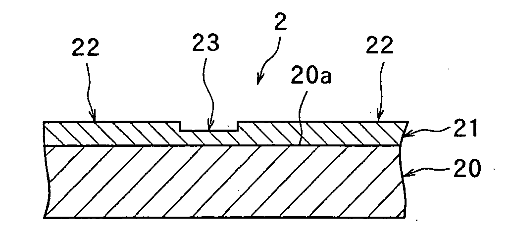
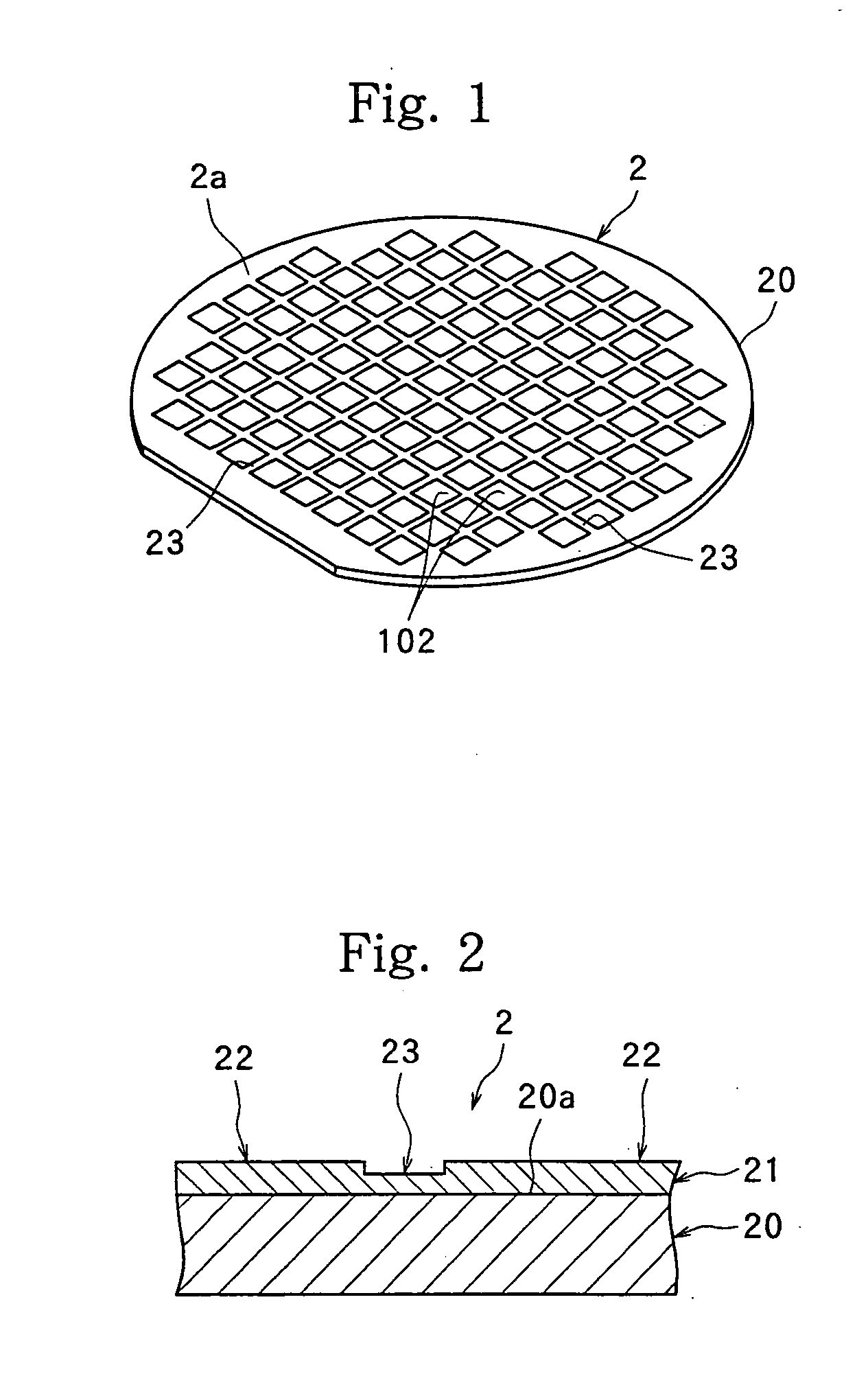
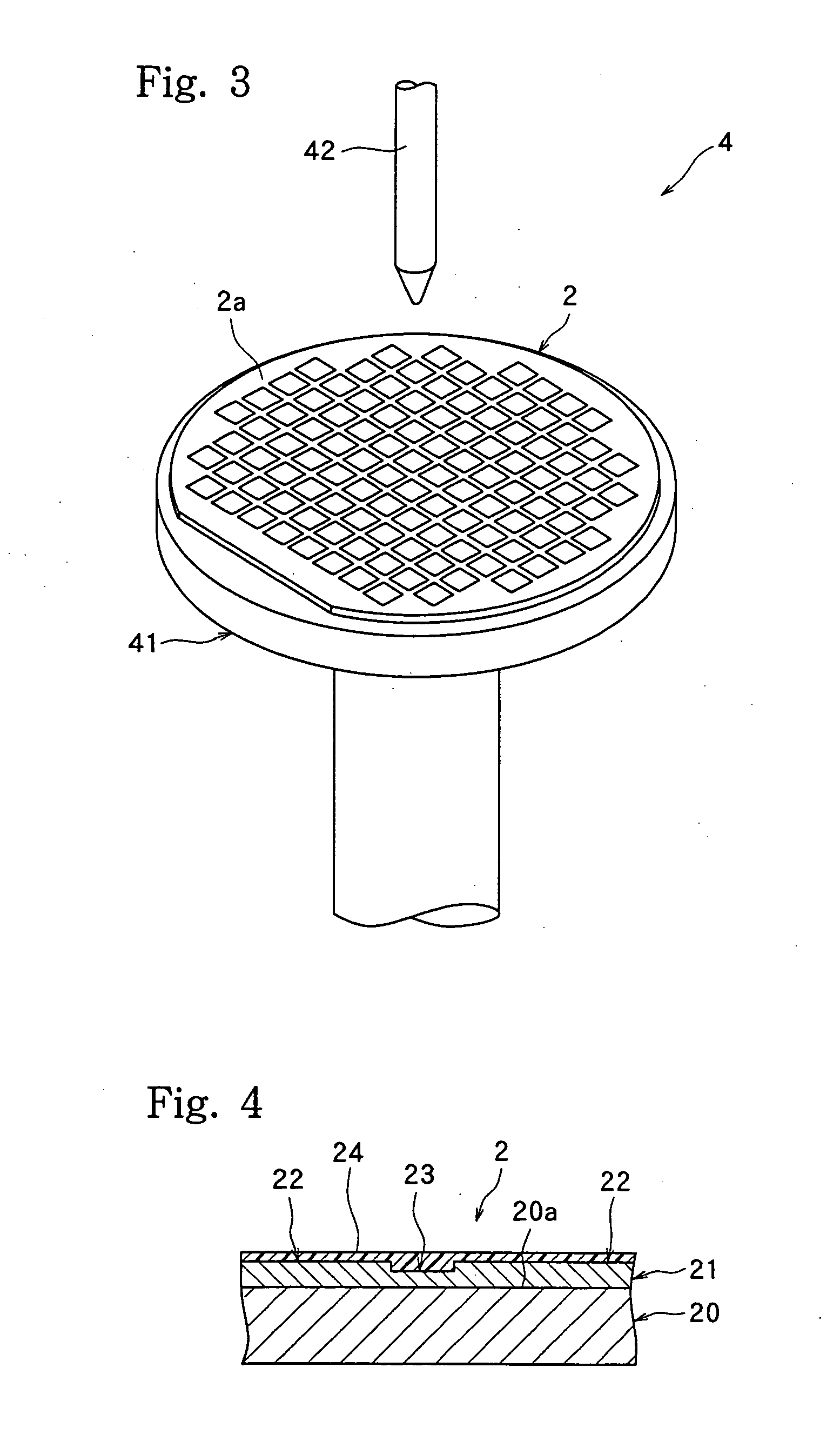
[0111] The above protective film agent was coated on a silicon wafer by a spinner, and dried to form a protective film having a thickness on the street of 0.5 to 1.5 μm. Then, the silicon wafer having the protective film formed thereon was mounted on the laser processing apparatus complying with the above specifications, and was subjected to laser processing. Then, the protective film was washed off with pure water, and the surroundings of the laser scans were observed. Bulges of the edge areas were observed, but no deposition of debris on the surroundings was noted. Thus, the silicon wafer was at a usable level. The width of processing w...

example 2

[0112] A protective film agent was prepared in exactly the same manner as in Example 1, except that the amount of ferulic acid, a water-soluble laser light absorber, was changed to 0.8 g. The g absorption coefficient k of the solids of the protective film agent was 5.61×10⁻¹.

[0113] Using the above protective film agent, a protective film having a thickness of 0.2 μm was formed on a silicon wafer in the same manner as in Example 1. Laser processing was performed in the same manner, and the protective film was washed off with water. Observation of the surroundings of the laser scans, which was made in the same manner as in Example 1, showed no deposition of debris. The width of processing was slightly larger than the laser spot diameter, but the silicon wafer was at a usable level.

example 3

[0114] A protective film agent was prepared in the same manner as in Example 1, except that polyvinyl alcohol having a saponification degree of 75% and a polymerization degree of 500 was used as the water-soluble resin. The g absorption coefficient k of the solids of the protective film agent was 1.56×10⁻¹ as in Example 1.

[0115] Using the above protective film agent, a protective film having a thickness of 0.5 to 1.5 μm was formed on a silicon wafer in the same manner as in Example 1. Laser processing was performed in the same manner, and the protective film was washed off with water. Observation of the surroundings of the laser scans, which was made in the same manner as in Example 1, showed no deposition of debris. The width of processing was comparable to the laser spot diameter without having influence from the thickness of the coating film.


PUM

PropertyMeasurementUnit
wavelengthaaaaaaaaaa
thicknessaaaaaaaaaa
grain sizeaaaaaaaaaa

Abstract

A protective film agent for laser dicing according to the present invention comprises a solution having, dissolved therein, a water-soluble resin and at least one laser light absorber selected from the group consisting of a water-soluble dye, a water-soluble coloring matter, and a water-soluble ultraviolet absorber. The protective film agent is coated on a surface of a wafer, which is to be processed, and is then dried to form a protective film. Laser dicing through the protective film produces chips from the wafer. As a result, deposition of debris can be effectively prevented on the entire face of the chips, including their peripheral edge portions.

Description

BACKGROUND OF THE INVENTION [0001] 1. Field of the Invention [0002] This invention relates to a protective film agent for use in laser dicing which applies a laser beam to a predetermined region of a wafer, such as a semiconductor wafer, to carry out predetermined processing, and a processing method by laser dicing using the protective film agent. [0003] 2. Description of the Related Art [0004] As is well known among those skilled in the art, a wafer formed in a semiconductor device manufacturing process has a laminate, which comprises an insulating film and a functional film stacked on the face of a semiconductor substrate, such as silicon, partitioned by a lattice of scheduled division lines, called streets. Respective regions partitioned by the streets define semiconductor chips such as IC's or LSI's. That is, a plurality of semiconductor chips are obtained by cutting the wafer along the streets. An optical device wafer has a laminate, which comprises a gallium nitride-based comp...

Claims


Application Information

Patent Timeline
Patent Type & Authority Applications(United States)
IPC IPC(8): H01L21/78
CPCB23K26/4075H01L21/67092C09D5/32B23K2201/40B23K2103/50B23K26/40B23K2101/40H01L21/82H01L21/78
Inventor TAKANASHI, HIROSHIKAWAKAMI, ATSUSHIYOSHIKAWA, TOSHIYUKIKITAHARA, NOBUYASU
Owner TOKYO OHKA KOGYO CO LTD
Why Eureka
Try Eureka