Method and apparatus for copper film quality enhancement with two-step deposition

a technology of copper film and two-step deposition, applied in the direction of electrical equipment, basic electric elements, semiconductor devices, etc., can solve problems such as performance reduction

Inactive Publication Date: 2006-05-18
TAIWAN SEMICON MFG CO LTD
View PDF11 Cites 24 Cited by
  • Summary
  • Abstract
  • Description
  • Claims
  • Application Information

AI Technical Summary

Benefits of technology

[0007] In one embodiment, the disclosure relates to a method for providing copper film quality enhancement with two-step deposition. The method includes providing a substrate; forming a trench in said substrate and depositing a conductive layer on said substrate. Optionally, a diffusion-barrier layer can be interposed between the substrate and the conductive layer that fills the trench. Next, an etch-stop layer can be deposited on the substrate followed by a dielectric layer. A trench having a via can be formed in the dielectric la...

Problems solved by technology

Voids can form within vias during metal deposition an cause reliability issues.
Small amounts of these ions are frequentl...

Method used


Image

  • Method and apparatus for copper film quality enhancement with two-step deposition
  • Method and apparatus for copper film quality enhancement with two-step deposition
  • Method and apparatus for copper film quality enhancement with two-step deposition

Examples


Embodiment Construction

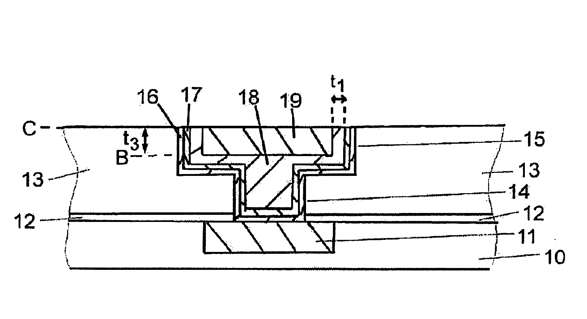
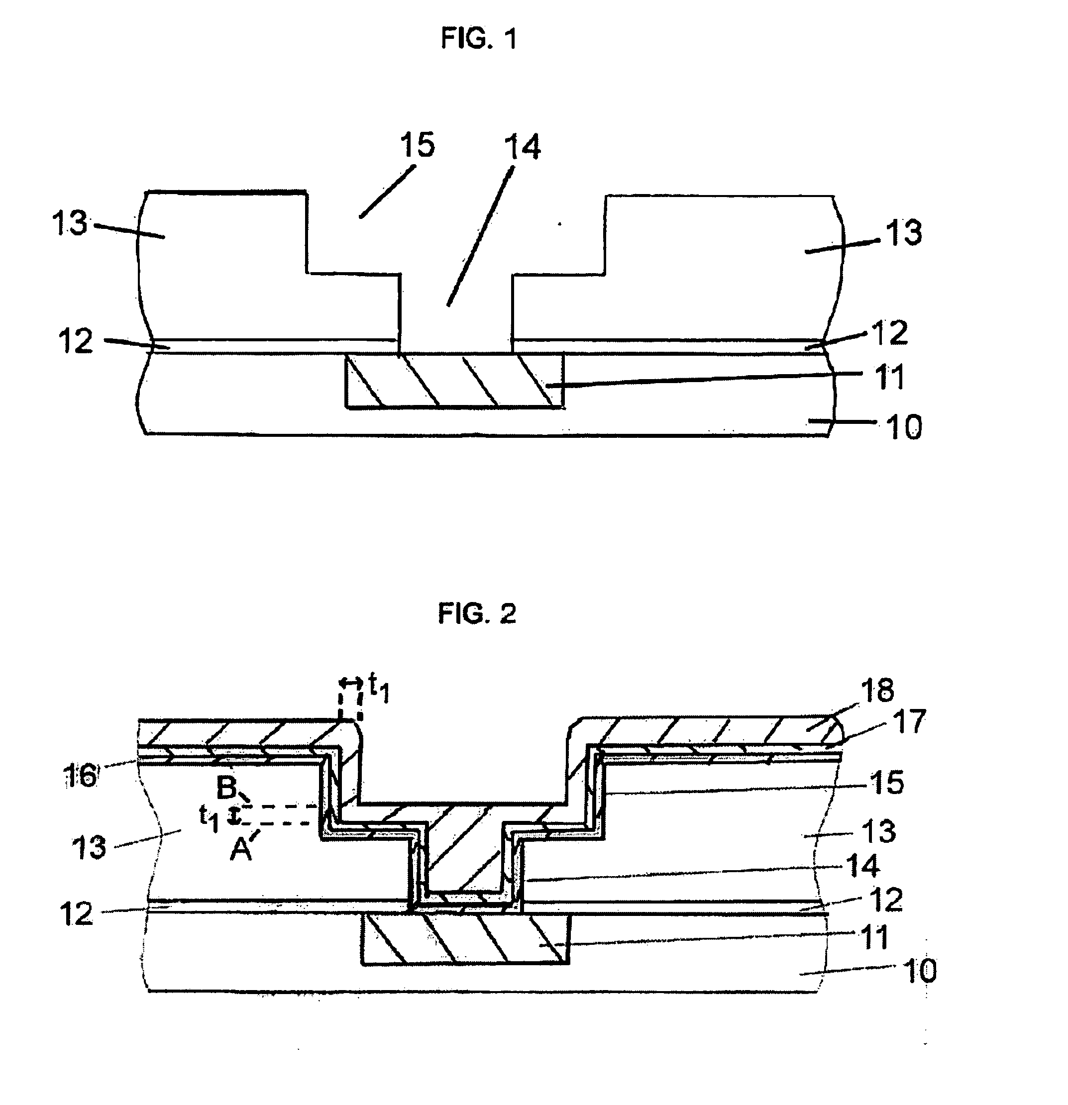
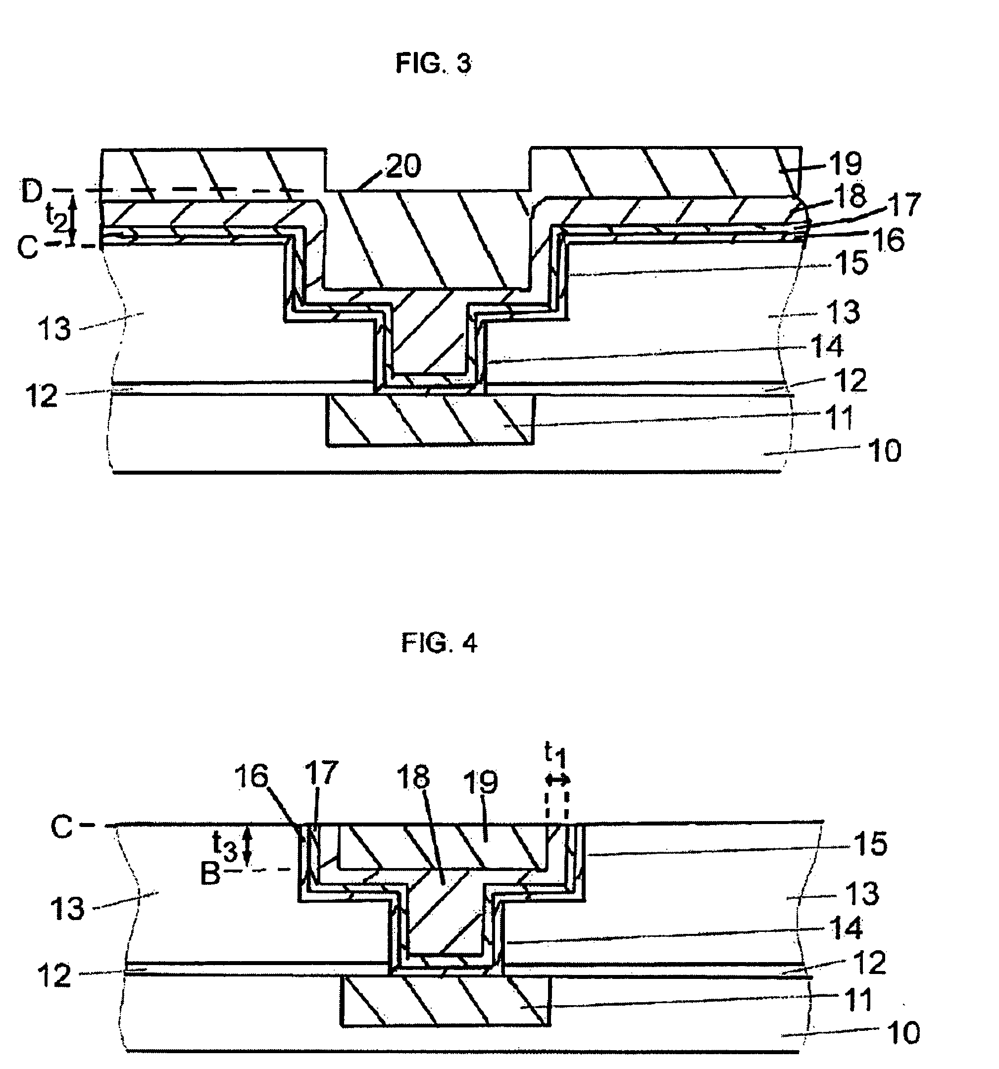
[0016]FIG. 1 is a schematic illustration of a substrate having a dielectric layer deposited thereon. In FIG. 1, a substrate 10 is provided that typically includes active and passive devices as well as conductive and dielectric layers that are not shown in order to simplify the drawing. Substrate 10 may include silicon or silicon-germanium, gallium-arsenide, or silicon-on-insulator technology. A conductive layer 11 is formed on substrate 10 by conventional means. Conductive layer 11 may include a metal such as AI, Cu, W, or an Al / Cu alloy. Optionally, conductive layer 11 is deposited on a diffusion barrier layer (not shown) within substrate 10 in order to protect the conductive layer from trace amounts of impurities in substrate 10 that may cause corrosion or oxidation of conductive layer 11. A diffusion barrier layer can also prevent metal ions in conductive layer 11 from diffusing into substrate 10 and diminishing the insulating capability of adjacent dielectric layers. The surface...


PUM

PropertyMeasurementUnit
Temperatureaaaaaaaaaa
Electrical conductoraaaaaaaaaa

Abstract

The disclosure relates to a method and apparatus for enhancing copper film quality with a two-step deposition. The two step deposition may include depositing a first copper film by electrochemical plating, annealing the first copper film at a desired temperature for a duration of time to remove any impurities, depositing a second copper film and annealing the second copper film for a duration of time to remove impurities. The second copper film can be deposited by electrochemical plating without HCl/C-based additive. The second copper film can also be deposited by sputtering to avoid impurities including C, Cl and S.

Description

[0001] The disclosure generally relates to a method and apparatus for providing copper interconnects with improved performance. BACKGROUND [0002] Copper has been used extensively in the electronics industry. Indeed, copper has been replacing aluminum as the basic metallization for integrated circuits (ICs). Copper provides a higher electroconductivity as compared, for example, with aluminum. Copper also has a higher resistance to electro-migration than aluminum, making copper a desirable replacement for aluminum. The higher electrical conductivity reduces resistive losses and provides for faster switching needed for advanced ICs. [0003] A well established process for fabricating copper circuitry on semiconductor chips is the so-called Damascene process. Under this process, vias are etched through and trenches are etched in the chip's dielectric material (typically silicon dioxide) although materials with lower dielectric constants are desirable. A barrier layer such as titanium nitr...

Claims


Application Information

Patent Timeline
IPC IPC(8): H01L21/4763H01L21/44
CPCC25D3/38C25D5/10C25D5/50H01L21/2885H01L21/76877C25D7/123
Inventor LIU, CHI-WENFENG, HSIEN-PINGTSAO, JUNG-CHIH
Owner TAIWAN SEMICON MFG CO LTD
Why Eureka
Try Eureka