Ifrared detector composed of group III-V nitrides

a nitride and infrared detector technology, applied in the field of infrared detectors, can solve the problems of limiting detector performance in practical applications, limiting the range of microbolometers and pyroelectric sensors, and affecting the accuracy of detectors, etc., to achieve the effect of improving sensitivity

Inactive Publication Date: 2006-05-25
MISSILE DEFENSE AGENCY CTS
View PDF18 Cites 39 Cited by
  • Summary
  • Abstract
  • Description
  • Claims
  • Application Information

AI Technical Summary

Benefits of technology

[0013] An object of the present invention is to provide a quantum-well infrared photodetector with improved sensitivity.
[0015] Another object of the present invention is to provide a quantum-well infrared photodetector having a lower cost as compared to arsenide-based devices.
[0020] First, the invention increases the electron effective mass thereby reducing leakage current. Current leakage has two primary sources, namely, thermionic emissions (TE), resulting from the direct excitation of electrons to the continuum band, and field-induced emissions (FIE), due to thermally assisted tunneling. TE leakage is reduced as it is inversely related to electron effective mass. Likewise, FIE leakage is reduced since tunneling probability is proportional to exp[−A(m*)½], where A is a constant related to barrier height and electric field and m* is the electron effective mass.
[0021] Second, the invention minimizes effects of dislocations and interfaces thereby achieving a higher quantum efficiency-mobility-lifetime product (ημτ product) than group IV, non-nitride group III-V, group II-IV and telluride-based compositions. Group III-V nitrides achieve a ημτ product in the range of 10−1 to 10 cm2 / V.
[0024] Fifth, the invention is easier to manufacture and process as compared to compositions including arsenic, mercury, and cadmium, and more environmentally friendly.

Problems solved by technology

However, microbolometers and pyroelectric sensors are resolution and range limited.
However, large format focal plane arrays suffer uniformity and operability problems in the range of LWIR.
However, material and surface problems limit detector performance in practical applications.
However, arsenide-based devices, such as those described and claimed by Gunapala et al. in U.S. Pat. No. 6,734,452 B2 and U.S. Pat. No. 6,211,529 B1, have a low quantum efficiency (10-20%), require cooling, and fail to detect infrared around 37 μm.
Both second and third generation devices are unable to absorb normal incident light.
However, both approaches increase complexity and cost and degrade performance by increasing crosstalk.
Furthermore, quantum well structures within diodes and lasers are simply too conductive for far infrared detection.

Method used


Image

  • Ifrared detector composed of group III-V nitrides
  • Ifrared detector composed of group III-V nitrides
  • Ifrared detector composed of group III-V nitrides

Examples


Embodiment Construction

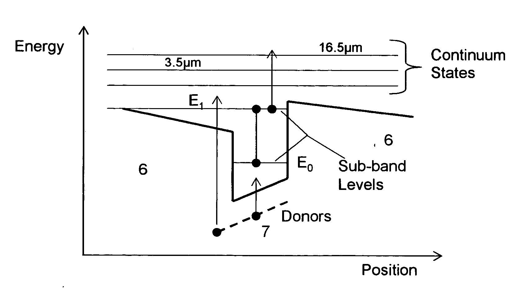
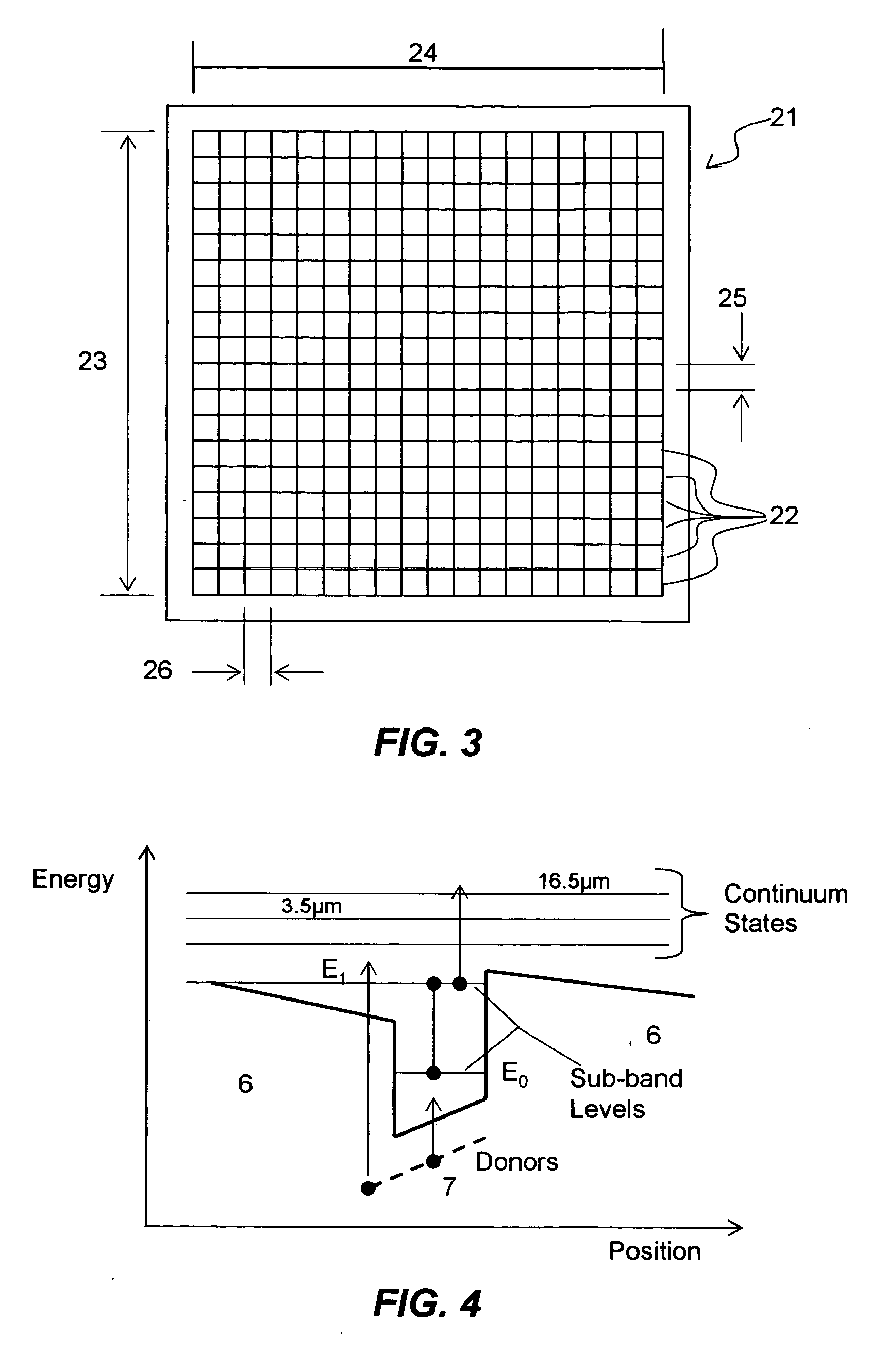
[0051]FIGS. 1 and 2 describe exemplary embodiments of the present invention. FIG. 3 describes the application of detectors 1 in FIGS. 1 and 2 to a focal plane array 21. FIG. 4 graphically represents the functional performance of devices shown in FIGS. 1 and 2. FIGS. 5 and 6 describe the performance of the present invention at near to long and very long wavelengths, respectively. Drawings are not to scale.

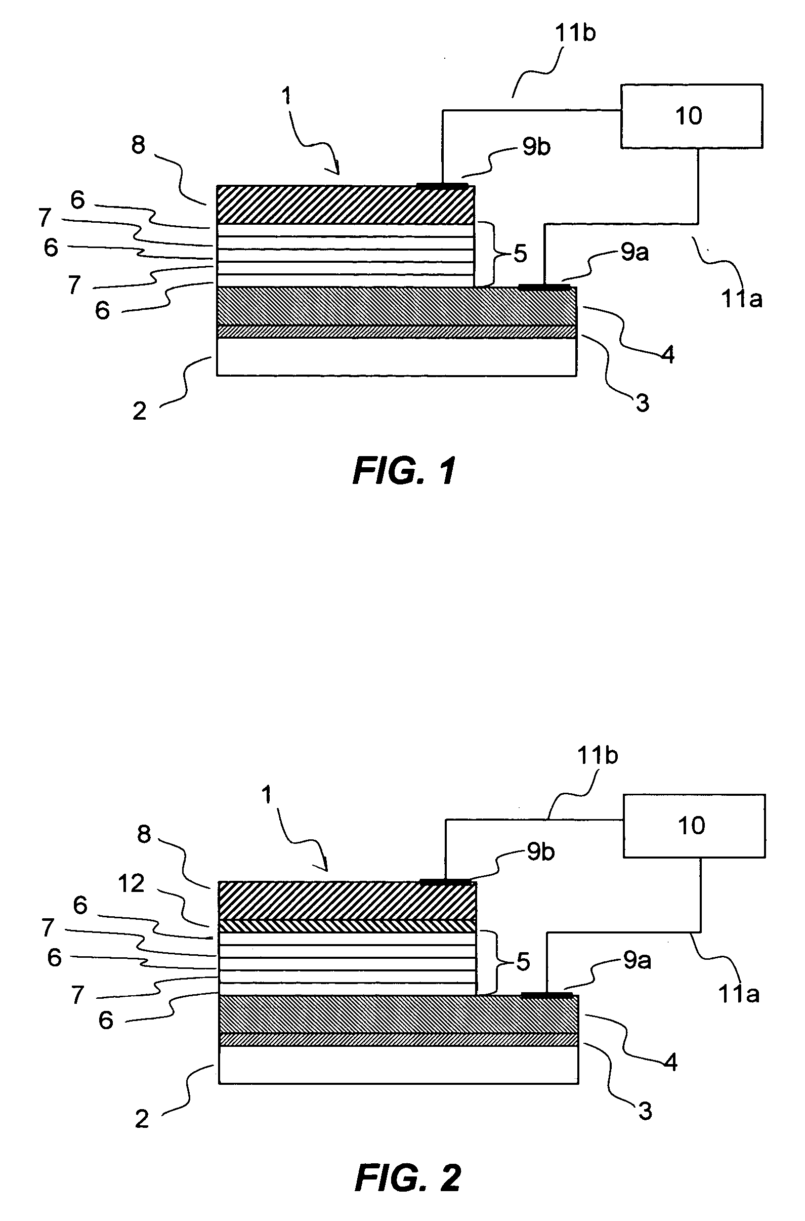
[0052] Referring now to FIG. 1, a detector 1 is shown having a substrate 2, a buffer layer 3, a first conducting layer 4, a multiple quantum well 5, and a second conducting layer 8. Layers are contacting and attached in the order described. Conductive contacts 9a and 9b are provided along one surface of the first conducting layer 4 and second conducting layer 8, respectively. Each contact 9a and 9b is thereafter electrically connected to a lead 11a and 11b, respectively. Leads 11a and 11b are electrically connected to a current sensing device 10. Leads 11a, 11b and current sensing ...


PUM

PropertyMeasurementUnit
infrared wavelengthsaaaaaaaaaa
quantum efficienciesaaaaaaaaaa
quantum efficiencyaaaaaaaaaa

Abstract

A quantum-well infrared photodetector (QWIP) is presented. The photodetector includes a substrate, a buffer layer, a first conductive layer, a multiple quantum well, an optional blocking layer, and a second conductive layer. Substrate is composed of a monocrystal which may be removed after fabrication. Remaining layers are composed of group III-V nitrides, including binary, ternary, and quaternary compositions. Alternate embodiments of the present invention include a doped binary alloy along first and second conductive layers, a binary alloy along buffer and blocking layers, and alternating alloys of binary, ternary and quaternary compositions within the multiple quantum well. The present invention responds to infrared light at normal and oblique incidences, from near infrared to very far infrared.

Description

FEDERALLY SPONSORED RESEARCH OR DEVELOPMENT [0001] This invention was made with government support under Contract No. DMI-0318901 awarded by the National Science Foundation. The United States Government has certain limited rights to at least one form of the invention.CROSS REFERENCE TO RELATED APPLICATIONS [0002] None. BACKGROUND OF THE INVENTION [0003] 1. Field of the Invention [0004] The present invention generally relates to an infrared detector having photocurrent responses from near infrared to very long wavelength infrared at normal and oblique incidences. Specifically, the invention is a quantum-well infrared photodetector composed of group III-V nitrides. [0005] 2. Description of the Related Art [0006] Infrared detectors are found in a wide variety of imaging applications, including night vision goggles, surveillance satellites, and seekers. Technical advances continue to increase the resolution and range of infrared systems and to lower their operational costs. [0007] Secon...

Claims


Application Information

Patent Timeline
Patent Type & Authority Applications(United States)
IPC IPC(8): G01J5/20
CPCB82Y20/00H01L27/14652H01L31/0304H01L31/03046H01L31/035236Y02E10/544Y10S977/759Y10S977/954Y10S977/816Y02P70/50
Inventor QIU, CHANG-HUA
Owner MISSILE DEFENSE AGENCY CTS
Why Eureka
Try Eureka