Organic photoelectric device with improved electron transport efficiency

a photoelectric device and electron transport technology, applied in the field of photoelectric devices, can solve problems such as inability to use in thermal evaporation process, and achieve the effect of increasing the electron transportability

Active Publication Date: 2006-05-25
OPTRONIC SCI LLC
View PDF18 Cites 23 Cited by
  • Summary
  • Abstract
  • Description
  • Claims
  • Application Information

AI Technical Summary

Benefits of technology

[0011] The present invention uses at least one layer of oxide-based alkali or alkaline-earth metal intercalation compound as a carrier transport layer in an organic optoelectronic device. In particular, the inserted layer is disposed between an electron injection layer or cathode and the organic sub-structure of the organic optoelectronic device in order to increase the transportability of electrons toward the organic sub-structure. Oxide-based alkali or alkaline-earth metal intercalation compounds are non-toxic and chemically stable. Furthermore, they can be deposited onto the optoelectronic device by the thermal evaporation process.
[0051] The third aspect of the present invention provides a method to improve operational efficiency of an optoelectronic device, the optoelectronic device comprising a first electrode, a second electrode and an organic optoelectronic sub-structure disposed between the first and the second electrodes, wherein the efficiency of the optoelectronic device is at least partially based on an electron transport process in the optoelectronic sub-structure. The method comprises the step of providing adjacent to the organic optoelectronic sub-structure an inorganic layer made substantially of a metal oxide doped with at least one electron-donating dopant, thereby enhancing the electron transport process, wherein the dopant is selected from the group consisting of alkali metals and alkaline-earth metals.

Problems solved by technology

However, because these types of dopant metals are chemically active, they may not be suitable for use in the thermal evaporation process that is commonly used in OLED manufacturing.

Method used


Image

  • Organic photoelectric device with improved electron transport efficiency
  • Organic photoelectric device with improved electron transport efficiency
  • Organic photoelectric device with improved electron transport efficiency

Examples


Embodiment Construction

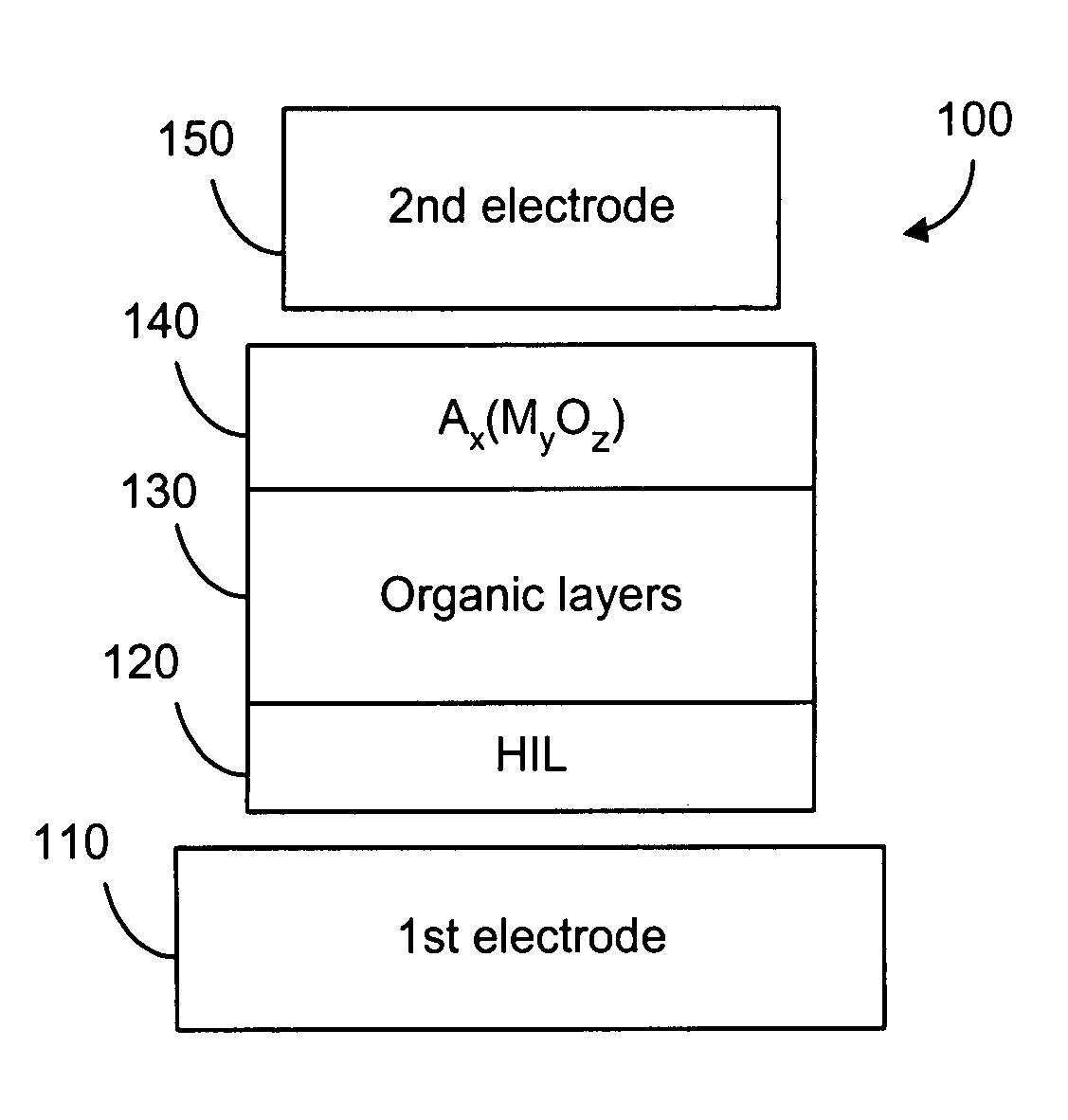
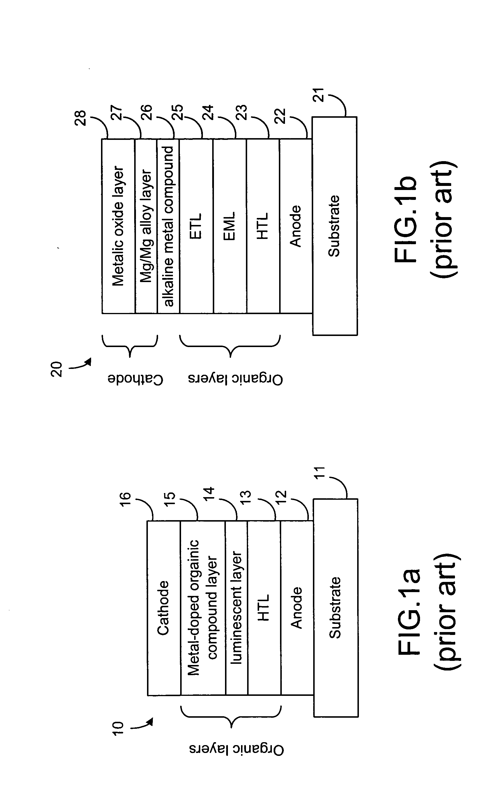
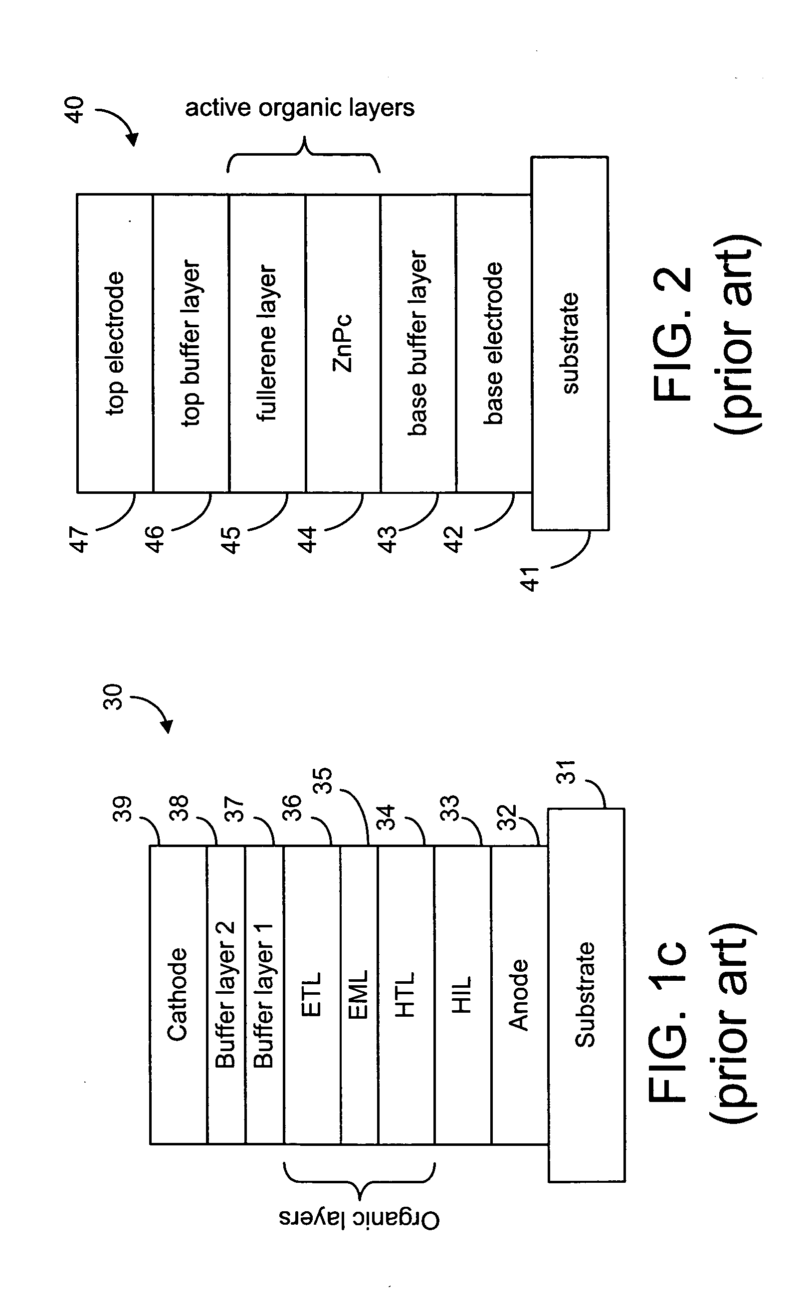
[0076]FIG. 3a is a schematic representation showing an embodiment of the present invention. As shown in FIG. 3a, an organic optoelectronic device 100 comprises a first electrode 110, a hole injection layer 120, a plurality of organic layers 130, a layer 140 of an oxide-based alkali or alkaline-earth metal intercalation compound and a second electrode 150. In general, the organic layers 130 comprise a hole transport layer, a luminescent layer and an electron transport layer, similar to the organic layers in prior art OLEDs as shown in FIGS. 1a to 1c. The organic layers 130 may comprise a fullerene layer and a phthalocyanine layer, similar to the organic layers in a prior art photocell, as shown in FIG. 2. In particular, the oxide-based alkali or alkaline-earth metal intercalation compound takes the form of a chemical formula Ax(MyOz), where x, y, z are positive integers greater than zero. The letter A represents an alkali or alkaline-earth element; M represents a metal, a transitiona...


PUM


Abstract

An opto-electronic device, such as an OLED or organic solar cell, having an electrode structure for use as a cathode. The electrode structure includes an electrically conductive layer and an inorganic layer, wherein the inorganic layer is made of at least one oxide-based alkali or alkaline earth metal intercalation compound. The intercalation compound having the chemical formula of Ax(MxOz), where x, y, z are positive integers greater than zero, A is an alkali metal or alkaline earth element, M is a metal, transitional metal or metallic alloy, and O is oxygen. Furthermore, a buffer layer made of alkali oxides or halides, or alkaline earth oxides or halides can be provided between the conductive layer and the inorganic layer.

Description

FIELD OF THE INVENTION [0001] The present invention relates generally to photoelectric devices and, more specifically, to organic light-emitting diodes and organic photocells. BACKGROUND OF THE INVENTION [0002] Organic light-emitting diodes (OLEDs) and organic photocells are structurally similar in that they all have an optoelectronic sub-structure disposed between two electrodes. The optoelectronic sub-structure is capable of converting electrical charge to light or converting photon energy to electrical charge. Typically at least one of the electrodes is made of a transparent material such as Indium Tin Oxide (ITO) so as to allow light to reach the optoelectronic sub-structure for photon to electric charge conversion or to allow light produced in the optoelectronic sub-structure to transmit therefrom. [0003] OLEDs are known in the art. For example, Hung et al. (U.S. Pat. No. 5,776,623) also discloses an electroluminescent device wherein a 15 nm-thick CuPc layer is used as an hole ...

Claims


Application Information

Patent Timeline
Patent Type & Authority Applications(United States)
IPC IPC(8): H01L29/08
CPCH01L51/0052H01L51/0078H01L51/0081H01L51/4206H01L51/424H01L51/441H01L51/50Y02E10/549H10K85/615H10K85/311H10K85/324H10K30/451H10K30/20H10K30/81H10K50/00
Inventor LIU, TSWEN-HSIN
Owner OPTRONIC SCI LLC
Why Eureka
Try Eureka