
Treating liquid for photoresist removal, and method for treating substrate

a technology of treating liquid and photoresist, which is applied in the direction of photomechanical treatment, photomechanical equipment, instruments, etc., can solve the problems of wiring delay, difficult to remove deteriorated films, and severe conditions, and achieve the effect of improving dissolution

Inactive Publication Date: 2006-05-25
TOKYO OHKA KOGYO CO LTD
View PDF0 Cites 16 Cited by
  • Summary
  • Abstract
  • Description
  • Claims
  • Application Information

AI Technical Summary

Benefits of technology

[0021] The present invention has been made in consideration of the above-mentioned situation, and its object is to provide a treating liquid for photoresist removal having the advantages in that it can greatly improve the dissolution (for promoted removal) of photoresist films deteriorated after dry-etching treatment, irrespective of the presence or absence of plasma-ashing treatment for them, that its effect is stable, that, even when used for substrates with copper wiring and a low-dielectric layer formed thereon, it does not have any negative influence on the dielectric constant of the dielectric layer, and that it has good corrosion resistance; and to provide a method for treating a substrate using the treating liquid.

Problems solved by technology

Recently, the treatment condition has become severer, and the deteriorated film has changed from an organic film to a film having an inorganic property, and it has become more difficult to remove the deteriorated film than before.
Further, the recent tendency in the art is toward the increase in the integration of semiconductor devices and the reduction in the size of chips, and therefore, wiring circuits are being much more micropatterned and multi-layered, and in that situation, some problems with semiconductor devices are pointed out such as wiring delay caused by the resistance of the metal layer used (wiring resistance) and the wiring capacity.
In addition, deposits that result from photoresist such as deteriorated photoresist films may also form.
Accordingly, if these deposits are not completely removed, then it causes a problem in that the yield in semiconductor production may lower.
It is said that the material of the type having such a low dielectric constant (low-k material) is poorly resistant to ashing or is not resistant to ashing, and when such a low-k material is used, a process not including a plasma-ashing step after dry-etching must be employed.
However, these cleaning liquid and removing liquid described in References 1 to 8 are still problematic in that, even when they are used, they could not attain the dissolution (for promoted removal) of deteriorated photoresist films, which the invention intends to attain, or since the stability of the liquids themselves is poor, they could not be used in practical production lines.
Reference 9 listed below discloses a photoresist-removing liquid comprising, as a water-soluble organic solvent therein, an aprotic polar solvent, propylene carbonate, which, however, is not still on a satisfactory level that is at present required in the field of production of more micropatterned and multi-layered semiconductor devices.

Method used


Image

  • Treating liquid for photoresist removal, and method for treating substrate
  • Treating liquid for photoresist removal, and method for treating substrate
  • Treating liquid for photoresist removal, and method for treating substrate

Examples


examples

[0069] The invention is described in more detail with reference to the following Examples, to which, however, the invention should not be limited. Unless otherwise specifically indicated, the amount is in terms of % by mass (substantial content, solid content). In Table 1, “PC” means propylene carbonate, and “PG” means propylene glycol.

1. Preparation of Photoresist-Stripping Liquid A:

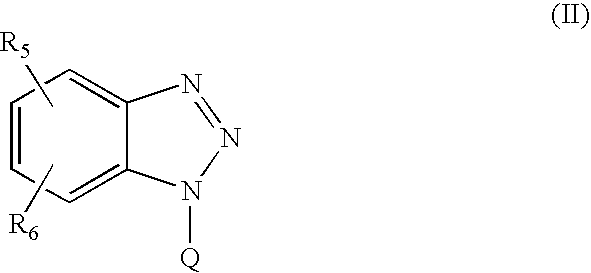
[0070] A photoresist-stripping liquid A was prepared according to an ordinary method, containing 10% by mass of tetramethylammonium hydroxide (TMAH), 57.5% by mass of dimethylsulfoxide (DMSO), 30% by mass of water, 1.5% by mass of thioglycerol and 1.0% by mass of 2,2′-{[(4-methyl-1H-benzotriazol-1-yl)methyl]imino}bisethanol (=“IR42”).

2. Production of Dry-Etched Substrate:

[0071] A positive photoresist, TDUR-P722 (by Tokyo Ohka Kogyo Co., Ltd.) was applied to a substrate having copper wiring formed thereon and having an SiOC layer (carbon-doped oxide layer; low-k layer) formed on it, and heated at 1...

examples 1 to 4

[0073] After dry-etched in the manner as above, the substrate was dipped in a treating liquid shown in Table 1, at 50° C. for 20 minutes, and then rinsed with pure water.

[0074] The surface of the thus-treated substrate was observed with SEM (scanning electronic microscope), and evaluated according to the following criteria. The results are shown in Table 1. The low-dielectric layer was not corroded.

[Dissolution (For Promoted Removal) of Deteriorated Photoresist Film]

[0075]◯: Effective for promoted removal of deteriorated photoresist film.

[0076] X: Not effective for promoted removal of deteriorated photoresist film.

[0077] Next, the substrate was dipped in the photoresist-stripping liquid A, at 50° C. for 20 minutes. Next, this was rinsed with pure water and then dried.

[0078] The surface of the thus-treated substrate was observed with SEM (scanning electronic microscope), and evaluated according to the following criteria. The results are shown in Table 1. The low-dielectric laye...


PUM


Abstract

Disclosed are a treating liquid for photoresist removal, containing (a) an oxidizing agent (e.g., aqueous hydrogen peroxide), (b) at least one selected from alkylene carbonates and their derivatives (e.g., propylene carbonate), and (c) water; and a method for treating with the treating liquid a substrate having a photoresist film deteriorated after dry-etching treatment thereof or a substrate optionally subjected to plasma-ashing treatment after the dry-etching treatment, and then treating it with a photoresist-stripping liquid for stripping off the photoresist.

Description

BACKGROUND OF THE INVENTION [0001] 1. Field of the Invention [0002] The present invention relates to a treating liquid for photoresist removal, which is used for removal of a photoresist film deteriorated after dry-etching treatment, and to a method for treating a substrate using the treating liquid. [0003] 2. Description of Related Art [0004] A semiconductor device, such as IC and LSI, is produced in the following process. A photoresist is uniformly coated on an electroconductive metallic film, an insulating film or a low dielectric material film formed on a substrate, such as a silicon wafer, by CVD vapor deposition process or the like. The photoresist is selectively subjected to exposure and development to form a photoresist pattern. The electroconductive metallic film, the insulating film or the low dielectric material film formed by CVD vapor deposition is selectively etched by using the photoresist pattern as a mask to form a minute circuit, and the photoresist layer thus beco...

Claims


Application Information

Patent Timeline
Patent Type & Authority Applications(United States)
IPC IPC(8): G03G13/00
CPCG03F7/423H01L21/31133
Inventor HARAGUCHI, TAKAYUKIWAKIYA, KAZUMASAYOKOI, SHIGERU
Owner TOKYO OHKA KOGYO CO LTD
Learn More