Self-aligned trench-type DMOS transistor structure and its manufacturing methods

a dmos transistor, self-aligned technology, applied in the direction of basic electric elements, electrical equipment, semiconductor devices, etc., can solve the problems of slow switching speed, improve the ruggedness of trench-type dmos transistors, improve gate-interconnection parasitic resistance, and improve source and p-base contact resistance.

Inactive Publication Date: 2006-06-01
SILICON BASED TECH
View PDF5 Cites 77 Cited by
  • Summary
  • Abstract
  • Description
  • Claims
  • Application Information

AI Technical Summary

Benefits of technology

[0013] The present invention discloses a self-aligned trench-type DMOS transistor structure and its manufacturing methods. The self-aligned trench-type DMOS transistor structure of the present invention comprises a self-aligned source structure in a self-aligned source region and a self-aligned trench gate structure in a trench gate region, in which the self-aligned source structure comprises a moderately-doped p-base diffusion region, a self-aligned n+ source diffusion ring, a self-aligned p+ contact diffusion region, and a self-aligned source contact window; the self-aligned trench gate structure comprises a self-aligned heavily-doped polycrystalline-silicon gate layer, a self-aligned heavily-doped polycrystalline-silicon gate layer capped with a self-aligned conductive layer formed between a pair of capping sidewall dielectric spacers, or a self-aligned trenched heavily-doped polycrystalline-silicon gate layer being filled with an etched-back conductive layer formed between a pair of capping sidewall dielectric spacers. The self-aligned n+ source diffusion ring is formed in a side surface portion of the moderately-doped p-base diffusion region, wherein the moderately-doped p-base diffusion region is formed by a p-diffusion region divided by the trench gate region and the self-aligned n+ source diffusion ring is formed by a n+ diffusion region divided by the trench gate region. The p-diffusion region is formed in the lightly-doped N− epitaxial silicon layer and the n+ diffusion region is formed in a surface portion of the p-diffusion region through a patterned window formed in the trench gate region. The self-aligned p+ contact diffusion region is formed by a self-aligned implantation window surrounded by a sidewall dielectric spacer formed over a sidewall of the trench gate region and on a side surface portion of a buffer oxide layer in the self-aligned source region. The self-aligned source contact window is formed in a self-aligned window surrounded by the sidewall dielectric spacer. The self-aligned trench-type DMOS transistor structure as described is fabricated by using only one masking photoresist step and exhibits the following advantages and features as compared to the prior arts: the self-aligned source region can be easily scaled down to have a minimum trench-type DMOS transistor size; the self-aligned n+ source diffusion ring and the self-aligned p+ contact diffusion region are heavily doped in a self-aligned manner to improve the source and p-base contact resistance and further to improve ruggedness of trench-type DMOS transistor; and a self-aligned highly conductive gate layer is used as a trench gate conductive layer to improve gate-interconnection parasitic resistance and a further scaling down of a trench width of the shallow trench can be easily obtained.

Problems solved by technology

Moreover, the parasitic resistance of the doped polycrystalline-silicon layer 114 as a gate metal layer is very large for gate interconnection of many trench-type DMOS transistor cells and may result in a slower switching speed.

Method used


Image

  • Self-aligned trench-type DMOS transistor structure and its manufacturing methods
  • Self-aligned trench-type DMOS transistor structure and its manufacturing methods
  • Self-aligned trench-type DMOS transistor structure and its manufacturing methods

Examples


Embodiment Construction

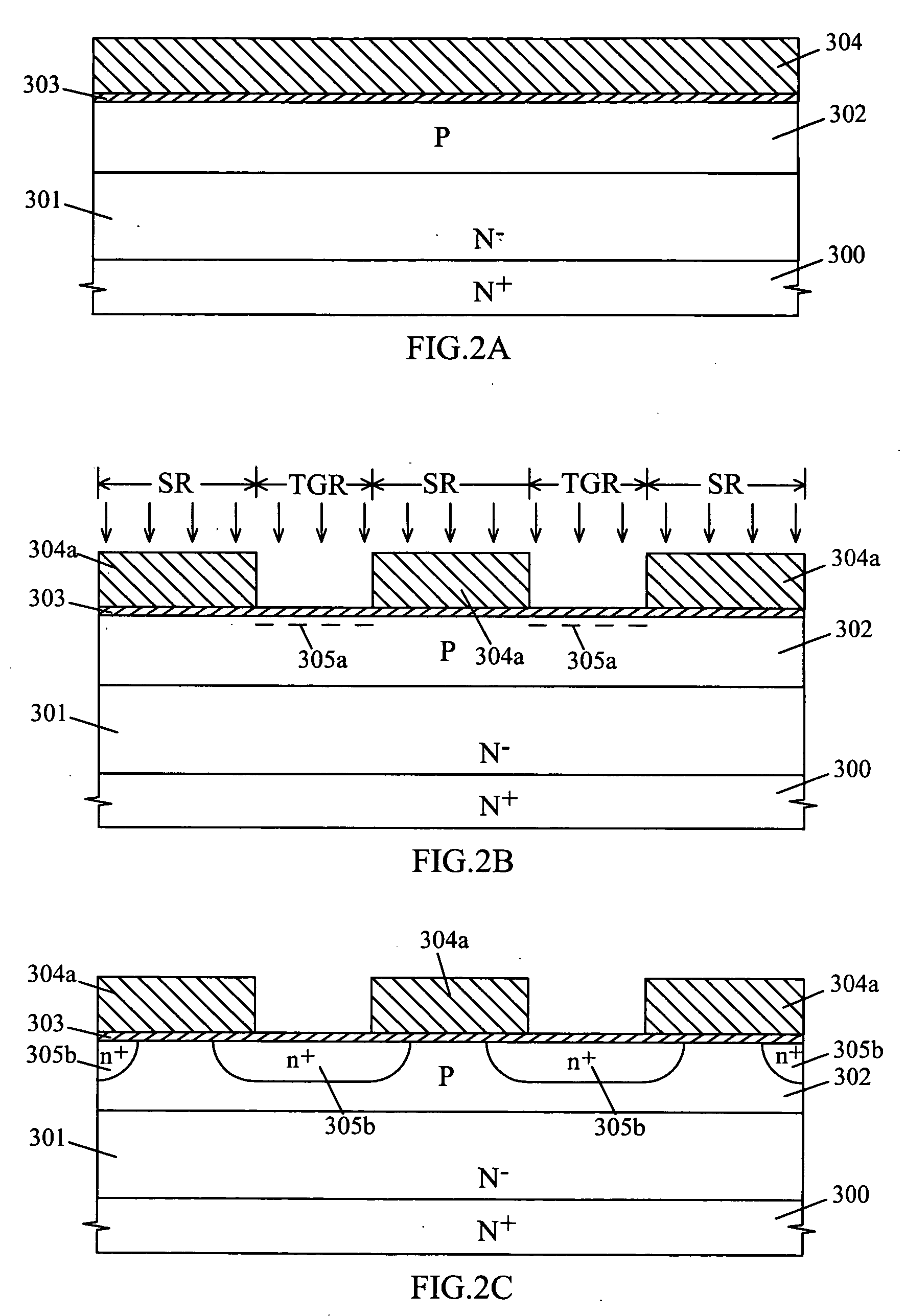
[0021] Referring now to FIG. 2A through FIG. 2H, there are shown process steps and their schematic cross-sectional views of fabricating a first-type self-aligned trench-type DMOS transistor structure of the present invention.

[0022]FIG. 2A shows that a lightly-doped N− epitaxial silicon layer 301 is formed on a heavily-doped N+ silicon substrate 300; a p-diffusion region 302 is formed on the lightly-doped N− epitaxial silicon layer 301; a buffer oxide layer 303 is formed on the p-diffusion region 302; and subsequently, a masking dielectric layer 304 is formed on the buffer oxide layer 303. The heavily-doped N+ silicon substrate 300 is preferably to have a resistivity between 0.001 *cm and 0.004 *cm and a thickness between 300 μm and 800 μm, depending on wafer size. The lightly-doped N− epitaxial silicon layer 301 is preferably to have a resistivity between 0.1 *cm and 100 *cm and a thickness between 1 μm and 100 μm. The p-diffusion region 302 is formed by boron ion-implantation with...


PUM


Abstract

The self-aligned trench-type DMOS transistor structure comprises a self-aligned source region being surrounded by a trench gate region. The self-aligned source region comprises a moderately-doped p-base diffusion region formed in a lightly-doped epitaxial semiconductor substrate, a self-aligned heavily-doped n+ source diffusion ring formed in a side surface portion of the moderately-doped p-base diffusion region, a heavily-doped p+ contact diffusion region formed in a surface portion of the moderately-doped p-base diffusion region surrounded by the heavily-doped n+ source diffusion ring, and a self-aligned source contact window formed by a semiconductor surface surrounded by a sidewall dielectric spacer. The trench gate region comprises a gate dielectric layer being lined over a trenched semiconductor surface with or without a thicker isolation dielectric layer formed on a bottom trenched semiconductor surface and a self-aligned highly conductive gate layer being formed at least over the gate dielectric layer.

Description

BACKGROUND OF THE INVENTION [0001] 1. Field of the Invention [0002] The present invention relates generally to a trench-type DMOS power transistor and its manufacturing method and, more particularly, to a self-aligned trench-type DMOS transistor structure and its manufacturing methods. [0003] 2. Description of the Prior Art [0004] A DMOS power transistor with very low on-resistance has become an important device for applications in battery protection, switching, linear regulator, amplifier and power management. Basically, the DMOS power transistor structure can be categorized into two groups: planar-type DMOS transistor structure and trench-type DMOS transistor structure. The planar-type DMOS transistor structure with MOS inversion channel being formed in a planar semiconductor surface, in general, exhibits a larger cell area and a larger turn-on resistance as compared to the trench-type DMOS transistor structure. Therefore, the trench-type DMOS transistor structure becomes a major ...

Claims


Application Information

Patent Timeline
Patent Type & Authority Applications(United States)
IPC IPC(8): H01L29/94
CPCH01L29/42368H01L29/456H01L29/4925H01L29/4933H01L29/66719H01L29/66734H01L29/7813
Inventor WU, CHING-YUAN
Owner SILICON BASED TECH
Why Eureka
Try Eureka