
Process for patterning capacitor structures in semiconductor trenches

a capacitor and trench structure technology, applied in the direction of semiconductor devices, electrical devices, transistors, etc., can solve the problems of high risk of incorrect processing, high deposition rate, and inability to meet the limits of technological feasibility, so as to reduce production costs and increase deposition rate

Inactive Publication Date: 2006-06-08
INFINEON TECH AG
View PDF10 Cites 16 Cited by
  • Summary
  • Abstract
  • Description
  • Claims
  • Application Information

AI Technical Summary

Benefits of technology

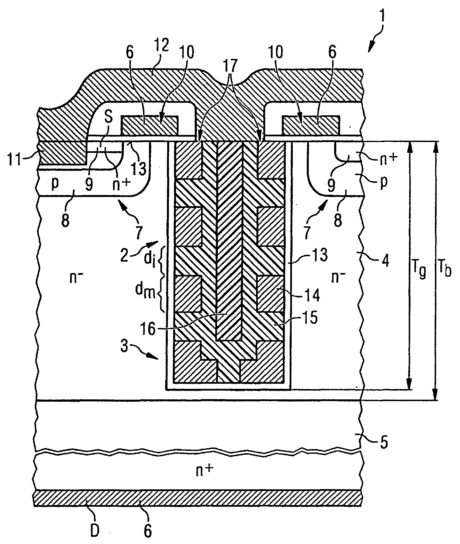
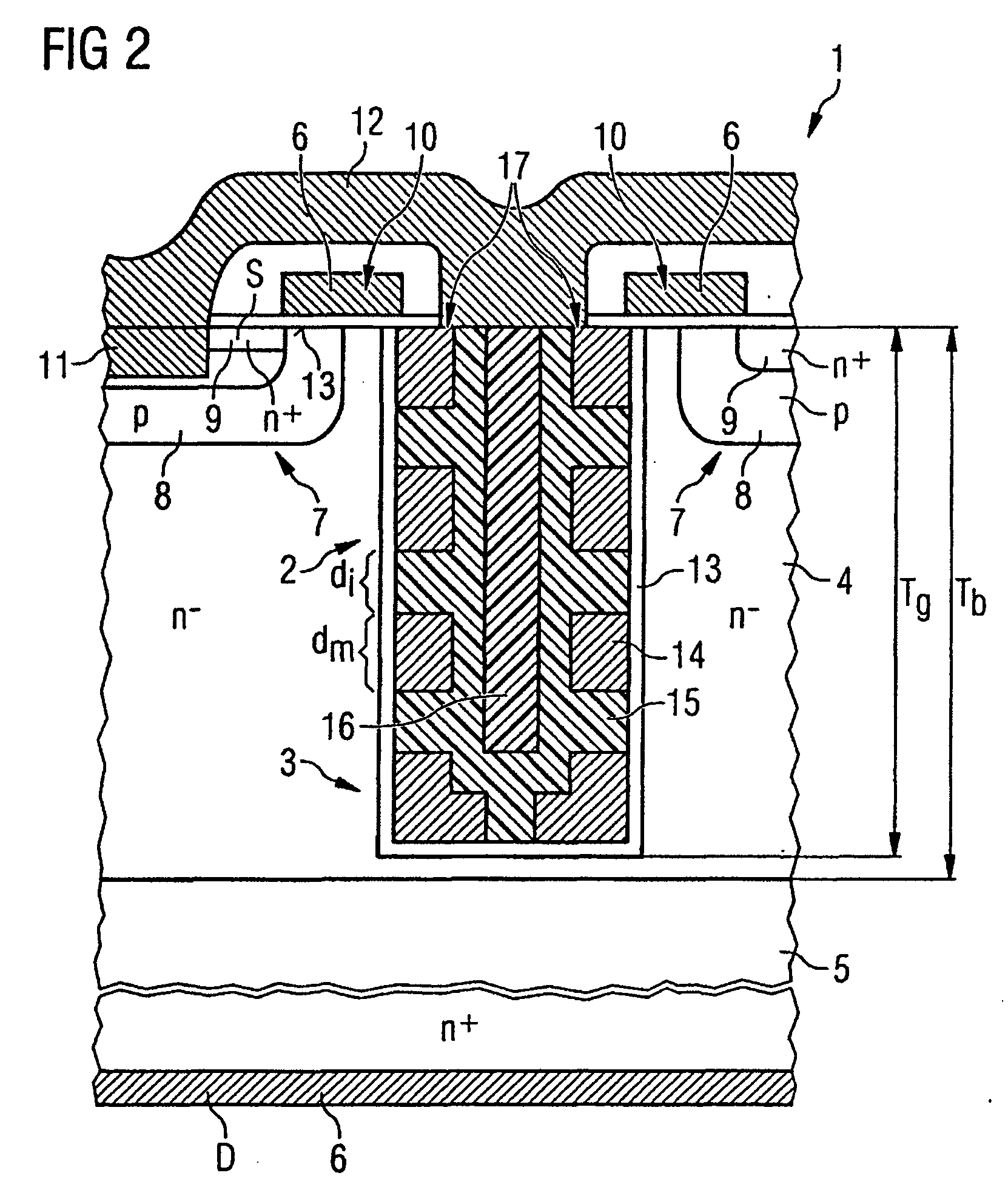
[0018] It is therefore possible to achieve a high effective relative permittivity εreff, especially since the effective relative permittivity includes the relative permittivity of the insulator multiplied by a factor derived from the ratio of the trench depth Tg to the sum of the thicknesses di of all the insulation layers between the islands in the trench. Accordingly, if the trench is 10 micrometers deep, for an εr of approximately 4, as is the case for example with silicon dioxide, the result is a sum of the thicknesses Σdi of all the insulation layers located above one another of just 40 nanometers if an effective permittivity of 1000 is to be achieved, but this leads to a low breakdown voltage. It is more favorable if an effective permittivity of only 200 is desired. This gives a thickness of 400 nm for the sum of the thicknesses di of the dielectric regions between the islands.
[0046] If, after the dielectric material has been deposited in the trench, the center of the trench, which remains clear, is filled with an oxide or imide, moisture is prevented from penetrating into the trench.

Problems solved by technology

Even nowadays, this is encountering the limits of technological feasibility.
The MOS field plate transistors comprising a trench structure which are known from U.S. Pat. No. 6,73,558 B2 have the disadvantage that, depending on the type of connection of the field plate, the entire reverse voltage is dropped either at the source end or at the drain end with respect to the n−-type zone, and therefore very thick insulation layers are required.
However, this process requires a large number of process steps, and consequently there is a high risk of incorrect processing.

Method used


Image

  • Process for patterning capacitor structures in semiconductor trenches
  • Process for patterning capacitor structures in semiconductor trenches
  • Process for patterning capacitor structures in semiconductor trenches

Examples


Embodiment Construction

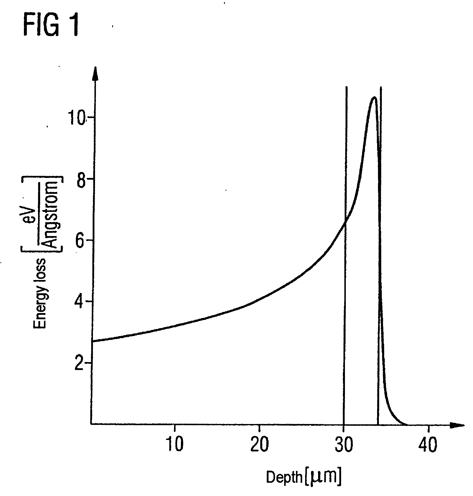
[0057] The starting point in the text which follows for describing the exemplary embodiment is a situation which results from FIG. 1 as described above. This figure is not described again at this point, for the sake of simplicity.

[0058]FIG. 2 shows a semiconductor component 1 with a trench 2 in which a capacitor structure 3 has been introduced. The semiconductor component 1 is a vertical power transistor which includes a drift zone 4 that consists of n−-doped semiconductor material and has a depth Tb. A drain zone 5 of n+-doped material with a metal drain electrode 6 is arranged below the drift zone 4. MOS structures 7 are located above the drift zone 4. These MOS structures include p-doped body zones 8, source zones 9 and gates 10. The source zones are connected to the metallic source electrode 12 by means of a metallic source contact. When a voltage which is higher than the threshold voltage of the semiconductor component 1 is applied, conducting channels 13 are formed in the bod...


PUM


Abstract

A process for producing structures in a semiconductor zone, has the steps of a) producing a trench (2) in the semiconductor zone (18), b) filling the trench with a photoresist (19), and c) exposing the photoresist (19) using ion beams (20), d) developing the photoresist (19). The energy density and ion dose for the ion beams (20) are selected in such a way that the photoresist (19) is only chemically changed at defined depths, so as to produce two regions, in the first region (21) of which the photoresist has been chemically changed at the defined depths by the ion beams (20), and in the second region of which the photoresist has been left chemically unchanged, so that during the developing step the photoresist is removed in precisely one of the two regions.

Description

CROSS-REFERENCE TO RELATED APPLICATIONS [0001] This application claims priority from German Patent Application No. 10 2004 054 352.6, which was filed on Nov. 9, 2004, and is incorporated herein by reference in its entirety. TECHNICAL FIELD [0002] The invention relates to a capacitor structure in trench structures of semiconductor components, to semi-conductor components comprising capacitor structures of this type, and to a process for patterning semiconductor components. BACKGROUND [0003] In conventional MOSFETs, the maximum donor concentration [ND] in an n−-type zone and therefore also the electrical conductivity of the n−-type zone are determined by the required blocking capability. In the event of an avalanche breakdown, approximately 1.5×1012 cm−2 donors are then ionized, the countercharge of which is found in the acceptor charge of the p-conducting zone of the MOSFET structure. If a higher donor concentration is to be made possible, countercharges for the donor atoms of the n−...

Claims


Application Information

Patent Timeline
IPC IPC(8): H01L29/94
CPCH01L27/1087H01L29/66181H10B12/0387
Inventor RUEB, MICHAEL
Owner INFINEON TECH AG
Learn More