Fin field effect transistor and method of manufacturing the same

a technology of fin fet and effect transistor, which is applied in the direction electrical apparatus, and semiconductor devices, can solve the problems of reducing the size of cmos devices to very small levels, affecting the operation of conventional cmos devices, and affecting the operation of basic electric elements, so as to achieve sufficient concentration of vertical gate fields and improve electrical characteristics of fin fet

Active Publication Date: 2006-06-08
SAMSUNG ELECTRONICS CO LTD
View PDF6 Cites 99 Cited by
  • Summary
  • Abstract
  • Description
  • Claims
  • Application Information

AI Technical Summary

Benefits of technology

[0028] Accordingly, the present invention provides a fin FET having a capping layer of which an original shape is maintained and having sidewall defects of a fin thereof that are mitigated or eliminated.
[0030] According to an aspect of the present invention, there is provided a fin field effect transistor that avoids the occurrence of damage at sidewalls of the fin. An active pattern protrudes in a vertical direction from a substrate and extends in a first horizontal direction along the substrate. A first silicon nitride pattern is provided on the active pattern. A first oxide pattern is provided on a surface of the substrate and on a sidewall of a lower portion of the active pattern, and a second silicon nitride pattern is provided on the oxide pattern. A device isolation layer is provided on the second silicon nitride pattern, so that a top surface of the device isolation layer is substantially coplanar with top surfaces of the oxide pattern and the second silicon nitride pattern. A buffer pattern is provided between the first oxide pattern and the second silicon nitride pattern, and the buffer pattern has an etching selectivity with respect to the second silicon nitride pattern.
[0056] According to the present invention, internal stresses that otherwise can be applied to sidewalls of the active pattern are sufficiently alleviated and an original shape of the first silicon nitride pattern, which is a capping layer of the active pattern, is maintained in an unchanged state throughout fabrication, so that concentration of the vertical gate field is sufficiently prevented and so that electrical characteristics of the fin FET are improved.

Problems solved by technology

However, as the size of CMOS devices continue to become reduced to very small levels, an effect known as a short channel effect can result as a consequence of the scaling-down of the gate size of the device.
This short-channel effect can degrade the performance of the CMOS device.
However, in such conventional CMOS devices, the characteristics of the device may be strongly influenced by the processing conditions used in fabricating the device when the gate length of the device is scaled down to less than about 50 nm, and conventional CMOS devices may break down completely and cease to operate as semiconductor circuits when the gate length of the device is scaled down to less than about 30 nm.
In addition, although the gate length of the device is scaled down, the occupying area for a unit cell is not scaled down because a spacer on a sidewall of a gate electrode is not reduced, so that the size reduction of the gate length does not necessarily contribute to increase in the degree of integration of a semiconductor device.
However, fabrication of conventional CMOS devices on SOI substrates may result in an increase in the parasitic resistance at the source / drain regions because the silicon layer of the SOI substrate is very thin, and thus a selective epitaxial growth step to form elevated source / drain regions may be included when fabricating transistors in SOI devices.
In addition, SOI devices may exhibit relatively poor contact with the substrate such that a floating body effect may arise and / or heat conduction between the device and the substrate may be reduced.
All of these effects may operate to reduce device performance.
However, the fin FET and the manufacturing method thereof have various associated problems.
As a result, electric characteristics of the transistor are deteriorated due to the concentration of the vertical gate field, such as swing degradation below a threshold voltage, decrease of threshold voltage and increase of current leakage below the threshold voltage.
However, the capping layer 120 is inevitably etched away by a certain amount despite the optimization of the etching conditions.
However, the above vertical channel fin FET has a problem in that sidewall defects of the fin caused by an etching process for the fin are hardly cured because the buffer oxide layer is formed by a CVD process.
The above non-cured sidewall defects of the fin may increase a charge trap on a gate insulation layer and deteriorate the quality of the gate insulation layer, thereby generating current leakage from the channel region.

Method used


Image

  • Fin field effect transistor and method of manufacturing the same
  • Fin field effect transistor and method of manufacturing the same
  • Fin field effect transistor and method of manufacturing the same

Examples


first embodiment

[0073]FIG. 7 is a perspective view illustrating a fin FET according to the present invention.

[0074] Referring to FIG. 7, the fin FET 300 of the first embodiment of the present invention includes a substrate 200a such as a silicon wafer, an active pattern 210, a first silicon nitride pattern 204a, a second oxide pattern 212a, a buffer pattern 214a, a second silicon nitride pattern 216a and a device isolation layer 218a. The fin FET 300 may further include a first oxide pattern 202a formed between the active pattern 210 and the first silicon nitride pattern 204a. When the first oxide pattern 202a is formed to a thickness below about 10 Å, a process for forming the first oxide pattern 202a is difficult to perform due to a small thickness thereof. When the first oxide pattern 202a is formed to a thickness over about 100 Å, notches on sidewalls of the first oxide pattern are so large that operation failures due to the notch are frequently generated. Accordingly, the first oxide pattern 2...

second embodiment

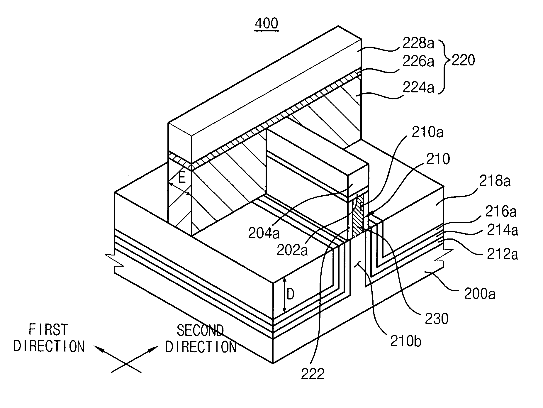
[0099] Referring to FIG. 19, the fin FET 400 of the present invention includes a substrate 200a such as a silicon wafer doped with P type impurities (hereinafter, referred to as P type substrate), an active pattern 210, a first silicon nitride pattern 204a, a second oxide pattern 212a, a buffer pattern 214a, a second silicon nitride pattern 216a and a device isolation layer 218a, a gate electrode 220 and a source / drain region 230 doped with N type impurities. The fin FET 400 may further include a first oxide pattern 202a formed between the active pattern 210 and the first silicon nitride pattern 204a.

[0100] The active pattern 210, which is known as a fin, protrudes from P type substrate 200a and extends in a first direction along the P type substrate 200a. The active pattern 210 includes a first portion 210a, which is not covered with the second oxide pattern 212a to be thereby exposed to surroundings and a second portion 210b that is covered with the second oxide pattern 212a. The...


PUM


Abstract

In a fin field effect transistor (FET), an active pattern protrudes in a vertical direction from a substrate and extends across the substrate in a first horizontal direction. A first silicon nitride pattern is formed on the active pattern, and a first oxide pattern and a second silicon nitride pattern are sequentially formed on the substrate and on a sidewall of a lower portion of the active pattern. A device isolation layer is formed on the second silicon nitride pattern, and a top surface of the device isolation layer is coplanar with top surfaces of the oxide pattern and the second silicon nitride pattern. A buffer pattern having an etching selectivity with respect to the second silicon nitride pattern is formed between the first oxide pattern and the second silicon nitride pattern. Internal stresses that can be generated in sidewalls of the active pattern are sufficiently released and an original shape of the first silicon nitride pattern remains unchanged, thereby improving electrical characteristics of the fin FET.

Description

CROSS-REFERENCES TO RELATED APPLICATIONS [0001] This application relies for priority upon Korean Patent Application No. 2004-100747 filed on Dec. 3, 2004, the content of which is herein incorporated by reference in its entirety. BACKGROUND OF THE INVENTION [0002] 1. Field of the Invention [0003] The present invention relates to a fin field effect transistor (FET) and a method of manufacturing the same, and more particularly, relates to a double gate fin FET and a method of manufacturing the same. [0004] 2. Description of the Related Art [0005] Complementary metal oxide silicon (CMOS) devices are widely used in various logic circuit applications such as central processing units and memory devices, and a great deal of added value can be generated in a CMOS-related industry. Accordingly, there has been intensive worldwide research has been conducted on CMOS devices based on nanotechnology. In many semiconductor device applications, the semiconductor device is required to exhibit low po...

Claims


Application Information

Patent Timeline
Patent Type & Authority Applications(United States)
IPC IPC(8): H01L21/338H01L29/76
CPCH01L29/66795H01L29/7851H01L29/7854H01L21/2254H01L21/2255H01L29/4232
Inventor LEE, DEOK-HYUNGSHIN, YU-GYUNLEE, JONG-WOOKKANG, MIN-GU
Owner SAMSUNG ELECTRONICS CO LTD
Why Eureka
Try Eureka