Field emission lighting device and method for making the same

Inactive Publication Date: 2006-06-15
HON HAI PRECISION IND CO LTD
View PDF7 Cites 9 Cited by
  • Summary
  • Abstract
  • Description
  • Claims
  • Application Information

AI Technical Summary

Benefits of technology

[0017] In addition, because the combined emitter tip and the emitter base have good mechanical strength, good electrical conductance, and excellent field-emission capability, the combined emitter tip and the emitter base may operate under relatively high-voltage electrical fields without the risk of being damaged.
[0018] A high-voltage electric field may be applied so as to obta

Problems solved by technology

The need for such a converter increases power consumption and the complexity of the configuration of the HID lamp.
Nevertheless, such metal or semiconductor ma

Method used


Image

  • Field emission lighting device and method for making the same
  • Field emission lighting device and method for making the same

Examples


Example

[0023] Embodiments of the present field emission lighting device will now be described in detail below and with reference to the drawings.

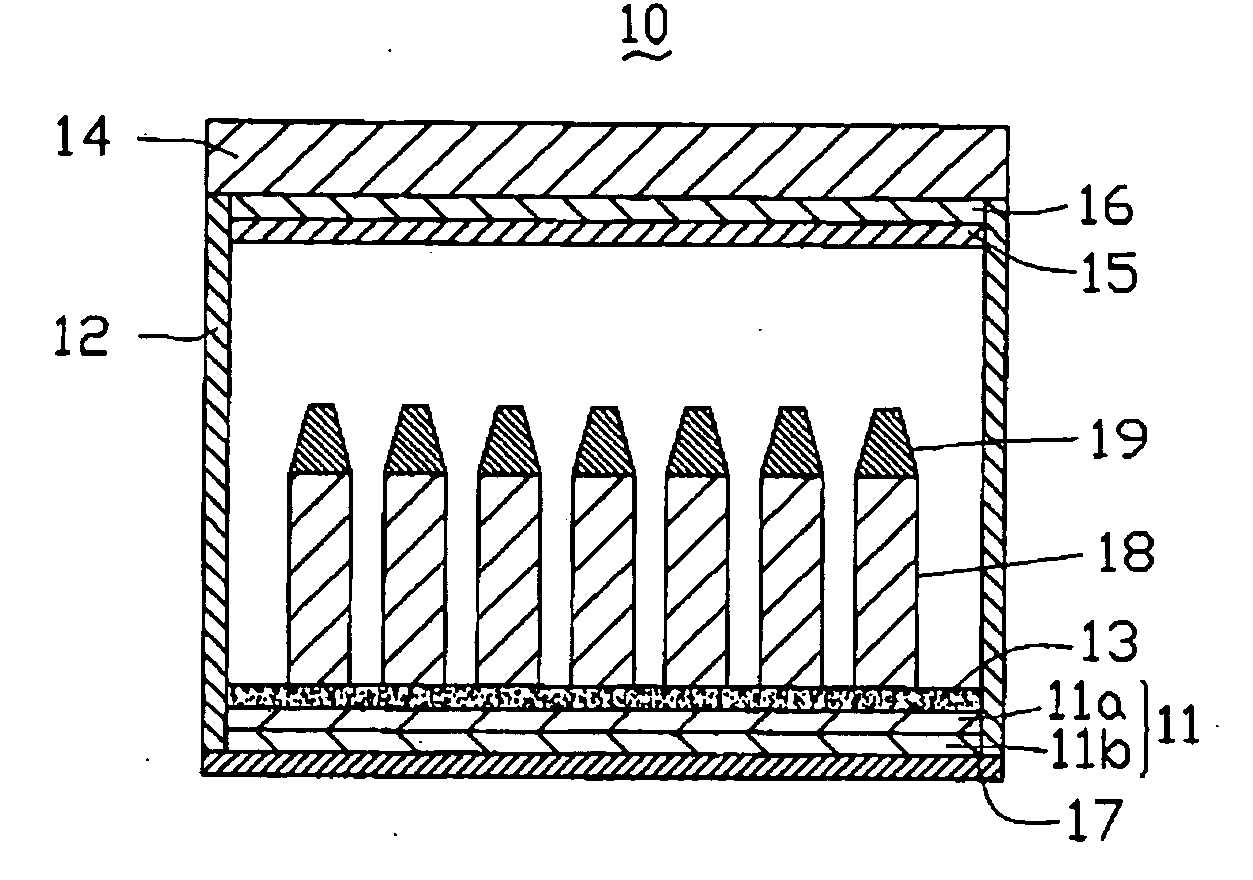
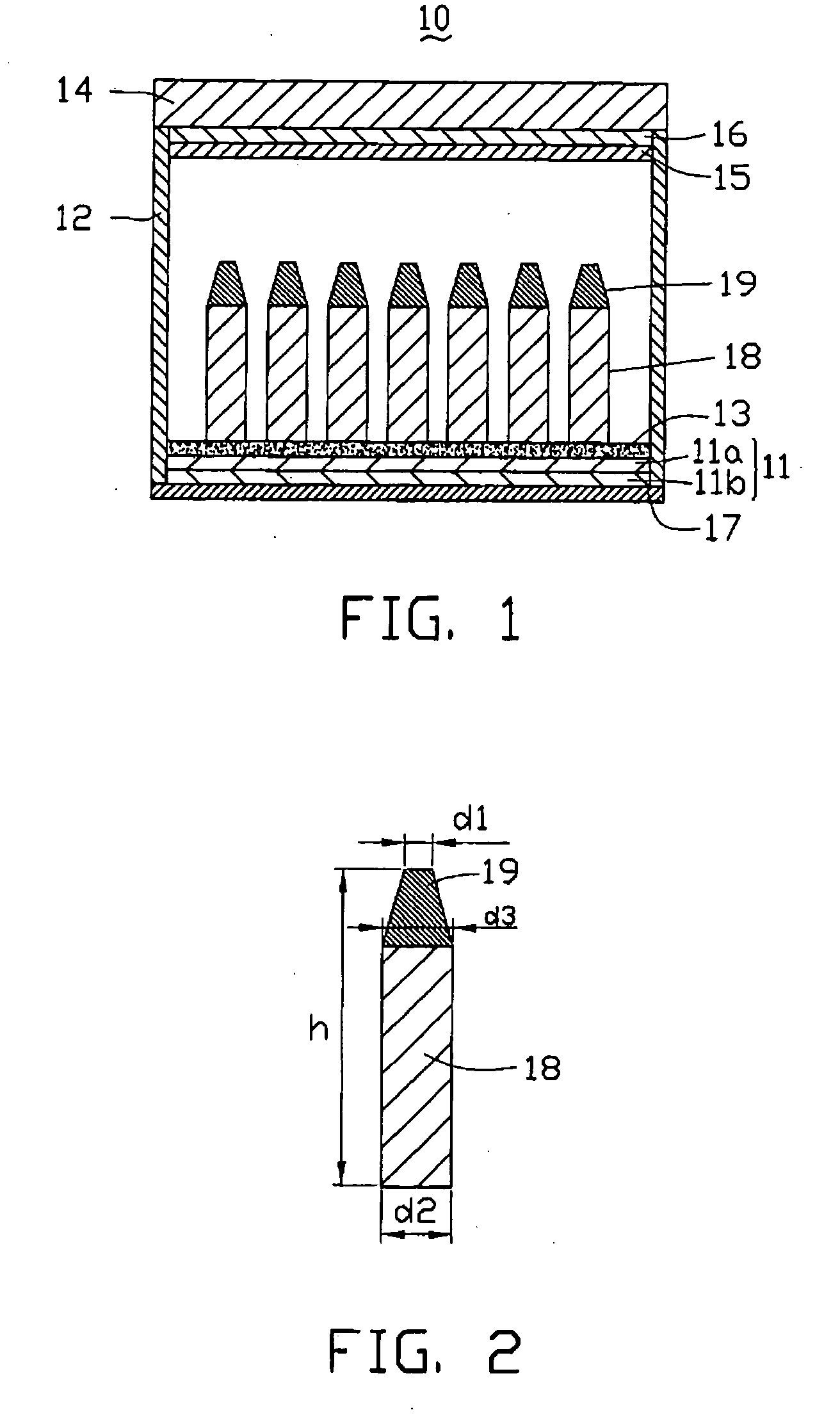
[0024]FIG. 1 illustrates a field emission lighting device 10 in accordance with a preferred embodiment. The field emission lighting device 10 mainly includes a cathode 11, a nucleation layer 13, a transparent upper substrate 14, a fluorescence layer 15, an anode 16, a low substrate 17, at least one electrically conductive emitter base 18, and at least one emitter tip 19. The cathode 11 is formed on the low substrate 17. The anode 16 is formed on an interior surface of the upper substrate 14. The fluorescence layer 15 is formed on the anode 16. The emitter base 18 is essentially made of diamond-like carbon (DLC). Each emitter tip 19 is formed on a respective emitter base 18.

[0025] The cathode 11 includes a cathode main body 11b and a functional layer 11a disposed on the cathode main body 11b. The cathode main body 11b is generally made, e.g., of ...


PUM


Abstract

A field emission lighting device and a method making the field emission lighting device are disclosed. The field emission lighting device includes a cathode, an anode, at least one emitter base, at least one conductive emitter tip, and a fluorescence layer. The emitter base is formed on the cathode and is made of diamond-like carbon. Each emitter tip is formed on a respective emitter base. The fluorescence layer is formed on the anode. In addition, each emitter tip has a bottom portion and a top portion. The bottom portion of the emitter tip has a cross-section size (i.e., diameter/width) essentially equal to the cross-section size of the emitter base. The emitter tip and the emitter base have a nanometer-magnitude size. The emitter base and a corresponding single emitter tip together form an emitter unit of the field emission lighting device.

Description

CROSS-REFERENCE TO RELATED APPLICATION [0001] This application is related to a copending U.S. patent application filed on Jul. 29, 2005 and entitled “FIELD EMISSION LIGHTING DEVICE” with the same assignee. The disclosure of the above-identified application is incorporated herein by reference.BACKGROUND [0002] 1. Field of the Invention [0003] The present invention relates to electronic lighting technology and, particularly, to a field emission lighting device and a method for making the field emission lighting device. [0004] 2. Discussion of the Related Art [0005] Conventional light sources generally include combustion-based light sources, incandescent light sources, and fluorescent light sources. The fluorescent light sources include, for example, high-intensity discharge (HID) lamps and light emitting diode (LED) lamps. [0006] As regards a typical HID lamp, a low voltage has to be converted into a high voltage of about 2300V so as to excite an inert gas to thereby produce electric ...

Claims


Application Information

Patent Timeline
IPC IPC(8): H01J1/02H01J9/02
CPCH01J9/025H01J63/02H01J63/06
Inventor CHEN, GA-LANE
Owner HON HAI PRECISION IND CO LTD
Why Eureka
Try Eureka